
- General Top
- SEMICONDUCTOR
- STORAGE
- COMPANY
-
My ToshibaSemicon
- Semiconductor Top
-
ApplicationsAutomotive
Body Electronics
xEV
In-Vehicle Infotainment
Advanced Driver-Assistance Systems (ADAS)
Chassis
IndustrialInfrastructure
BEMS/HEMS
Factory Automation
Commercial Equipment
Consumer/PersonalIoT Equipment
Healthcare
Wearable Device
Mobile
Computer Peripherals
-
ProductsAutomotive Devices
Discrete Semiconductor
Diodes
Transistors
Logic ICs
Analog Devices
Digital Devices
Wireless Devices
※
 : Products list (parametric search)Power Semiconductors
SiC Power Devices
※
: Products list (parametric search)Isolators/Solid State RelaysPhotocouplers
Digital Isolators
Solid State Relays
Fiber Optic Transmitting Modules
※
: Products list (parametric search)MOSFETsIGBTs/IEGTsBipolar Transistors※
: Products list (parametric search)Diodes※
: Products list (parametric search)MicrocontrollersMotor Driver ICsIntelligent Power ICs※
: Products list (parametric search)Power Management ICsLinear ICs※
: Products list (parametric search)General Purpose Logic ICsLinear Image SensorsOther Product ICsOther Product ICs
※
: Products list (parametric search) -
Design & Development
-
Knowledge
- Where To Buy


- Part Number & Keyword Search
- Cross Reference Search
- Parametric Search
- Stock Check & Purchase
This webpage doesn't work with Internet Explorer. Please use the latest version of Google Chrome, Microsoft Edge, Mozilla Firefox or Safari.
require 3 characters or more. Search for multiple part numbers fromhere.
The information presented in this cross reference is based on TOSHIBA's selection criteria and should be treated as a suggestion only. Please carefully review the latest versions of all relevant information on the TOSHIBA products, including without limitation data sheets and validate all operating parameters of the TOSHIBA products to ensure that the suggested TOSHIBA products are truly compatible with your design and application.Please note that this cross reference is based on TOSHIBA's estimate of compatibility with other manufacturers' products, based on other manufacturers' published data, at the time the data was collected.TOSHIBA is not responsible for any incorrect or incomplete information. Information is subject to change at any time without notice.
require 3 characters or more.
3.2. Common-mode input voltage range (CMVIN) and common-mode input signal rejection ratio (CMRR)

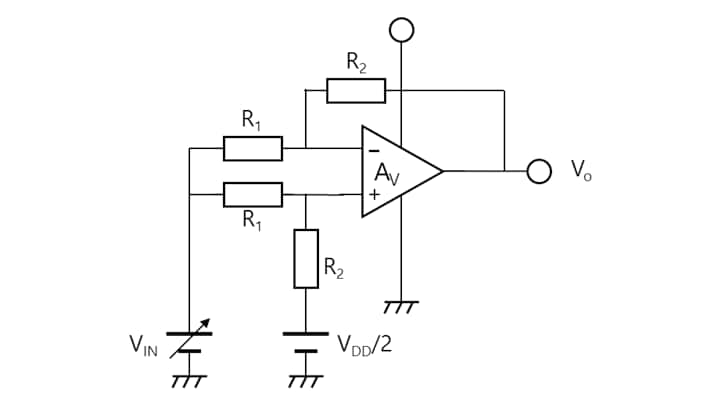
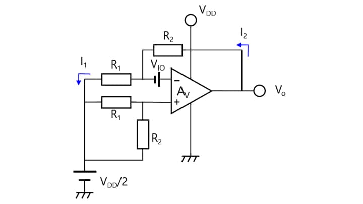
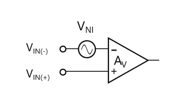
The common-mode input signal rejection ratio (CMRR) of a differential amplifier is a metric used to indicate its ability to reject two signals or noises (common-mode noise) that have the same amplitude and phase at VIN(-) and VIN(+). It is expressed by the following equation. Figure 3-5 shows a test circuit for the common-mode input signal rejection ratio.
The common-mode input voltage range (CMVIN) is defined as the input voltage range in which the prescribed CMRR is satisfied under the prescribed conditions. The datasheets for Toshiba’s op-amps specify the CMRR value under DC conditions.
where VIN1 and VIN2 are the maximum and minimum CMVIN values, respectively, and VOUT1 and VOUT2 are the output (VO) voltages at VIN1 and VIN2, respectively.
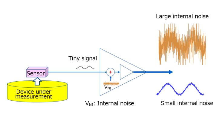
As can be seen from Figure 3-5, the input offset voltage (VIO) discussed in the previous section is the CMRR value under a special condition (VIN = VDD/2).
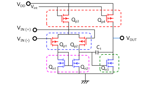
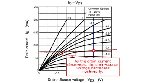
The op-amp operates as described in Section 1.2. The differential input pair of a typical op-amp is composed of P-channel MOSFETs as shown in Figure 3-6. As the VIN(+) and VIN(-) voltages increase, the drain-source voltage of Qp3 in the current source decreases, causing the current flowing to the differential input pair and the current mirror to decrease slightly. Figure 3-7 shows an example of ID-VDS curves for a discrete P-channel MOSFET. Suppose, for example, that VDS = -1.5 V and ID = 80 mA initially. As the drain current of the MOSFET decreases, its drain-source voltage changes nonlinearly in the saturation region.
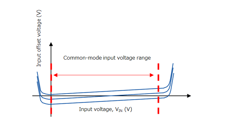
Although the internal devices of an op-amp IC are placed and fabricated in such a manner as to make the MOSFETs uniform, they are not perfectly symmetrical at the micro level. In addition, semiconductor chips are mounted on a metal frame in a package and soldered onto a printed circuit board. Therefore, the mechanical stress applied to each element of an op-amp IC differs slightly. These factors cause a slight difference in threshold voltage among the P-channel MOSFETs of the differential input pair. Therefore, a decrease in drain current causes different nonlinear changes in their drain-source voltage. As a result, the input offset voltage has a slope with respect to the input voltage (VIN) in the common-mode input voltage range as shown in Figure 3-8. Therefore, the CMRR values are calculated at the maximum and minimum common-mode input voltages.
Related information
Chapter3 Electrical characteristics
Related information
- Products
- Application Notes
- FAQs
- Parametric Search
- Stock Check & Purchase