What are the characteristics of Schottky barrier diodes (SBDs)?
Forward voltage is smaller than that of a general diode, but reverse current (leak current) becomes bigger. There is a trade-off between forward voltage and reverse current.
SBDs have the following advantages and disadvantages compared with pn junction diodes (PNDs):
Advantages:
- Low forward voltage (VF)
- High switching speed (extremely low reverse recovery time)
Disadvantages:
- Large leakage current
- Low reverse withstand voltage
A pn junction diode formed by a junction of p-type and n-type semiconductors works as a diode because of a junction barrier created by an electric potential difference between the two semiconductors.
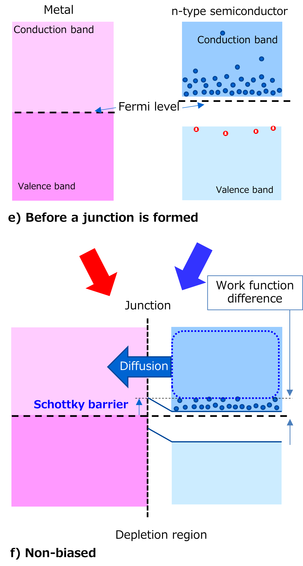
In contrast, an SBD formed by a junction of a semiconductor (typically an n-type semiconductor) and a metal such as platinum (Pt), molybdenum (Mo), and titanium (Ti) works as a diode because of a Schottky barrier created by a difference in their work functions*. Before the junction of an SBD is formed, the conduction band of the metal is filled with electrons up to the Fermi level as shown in Fig. e). Therefore, when the metal is joined, for example, with an n-type semiconductor, holes, which are minority carriers for the n-type semiconductor, do not exist in it because they combine with electrons in the metal as shown in Fig. f). This means that only electrons contribute to current. For this reason, SBDs are called unipolar devices.
SBDs exhibit only extremely short reverse recovery time** because of the absence of minority carriers whereas reverse recovery time poses a concern for pn junction diodes.
This makes SBDs suitable for high-speed switching applications.
The magnitude of the potential barrier (Schottky barrier) that determines the forward voltage of the SBD depends on a difference between the work function of the metal and the electron affinity of the semiconductor. Reducing this difference helps reduce the diode turn-on forward voltage (VF or VFM) as Fig. 1.
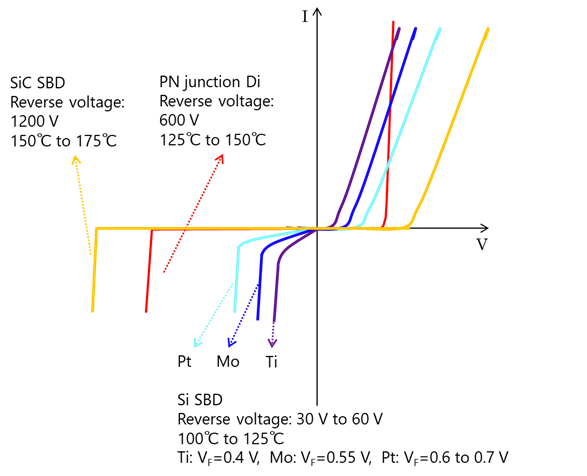
In the case of bipolar devices such as pn junction diodes, conductivity modulation is used to reduce VF in the high-current region. However, since conductivity modulation does not occur in an SBD which is unipolar device, the resistance in the drift region decreases. In other words, the dopant concentration in its drift region must be higher than that of a typical pn junction diode. The resulting downside of SBDs is low reverse withstand voltage (VR or VRRM). Toshiba now offers SBDs fabricated using silicon carbide (SiC), a wide-bandgap semiconductor, instead of silicon. Because of a higher bandgap and bond strength than silicon, SiC provides a 10 times higher electric breakdown field than silicon. As a result, SiC SBDs are available with a withstand voltage of 650 V or higher whereas silicon SBDs, in practice, provide a withstand voltage of only 150 V or so.
* Work function: Energy needed to remove an electron from the surface of a metal. In the case of silicon and other semiconductors, the work function represents electron affinity.
** The reverse recovery time of SBDs is not zero because of the presence of a pn junction in the guard ring region and parasitic capacitance. Although SBDs exhibit reverse recovery time, it is much shorter than that of pn junction diodes.
pn junction diode
A pn junction diode is a type of diode formed by the junction of p-type and n-type semiconductors. The energy structures of p-type and n-type semiconductors are shown at right.
a) Before a junction is formed
(i.e., when p-type and n-type sides are separate):
The band diagram of the p-type semiconductor shows that it has a high concentration of holes, majority carriers, in the valence band and a low concentration of electrons, minority carriers, in the conduction band. Conversely, the n-type semiconductor has a high concentration of electrons, majority carriers, in the conduction band and a low concentration of holes, minority carriers, in the valence band. The Fermi level (i.e., the energy level that has a 50% probability of being occupied by majority carriers) is close to the valence band in the case of the p-type semiconductor and to the conduction band in the case of the n-type semiconductor.
b) Non-biased state
(i.e., when a junction is formed by the p-type and n-type semiconductors but is not biased)
When the p-type and n-type semiconductors are joined together to form a pn junction, band bending occurs near the junction, causing their Fermi levels to become equal. At this time, a Schottky barrier is created because of a difference in an electric potential between the p-type and n-type semiconductors. This makes it difficult for the holes in the p-type side and the electrons in the n-type side to diffuse into the other side of the junction.
Only holes and electrons existing in an energy state greater than the Fermi level diffuse from areas of high concentration to areas of low concentration so that they are evenly distributed.
The depletion region extends around the junction. Its width is inversely proportional to the concentration of p-type and n-type impurities.

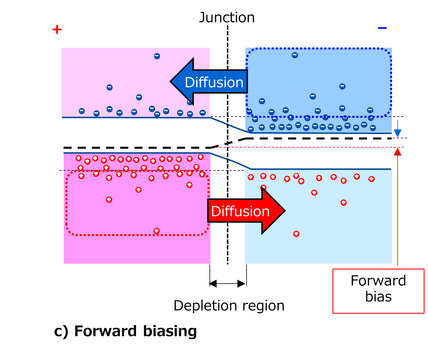
c) Forward-biased state
(i.e., when the p-type side is more positively biased than the n-type side)
The Fermi level of the n-type semiconductor increases by the amount of forward bias, causing the potential barrier to decrease. As a result, the number of holes and electrons with energy greater than the potential barrier increases exponentially, causing diffusion current to flow. The depletion region around the junction shrinks.
d) Reverse-biased state
(i.e., when the n-type side is more positively biased than the p-type side)
The Fermi level of the n-type semiconductor decreases by the amount of reverse bias, causing the potential barrier to increase. As a result, the number of holes and electrons with energy greater than the potential barrier decreases exponentially. The depletion region around the junction widens.

Schottky barrier diode
A Schottky barrier diode (SBD) is a type of diode that has a junction formed between a semiconductor (typically an n-type semiconductor) and a metal.
e) Before a junction is formed
(i.e., when p-type and n-type semiconductors are separate):
Semiconductors have an empty band above the band gap. Valence electrons become conduction electrons when they acquire the energy needed to jump into the conduction band. The electrons in a metal can move freely among atoms because the band in which valence electrons exist has an empty energy level. Therefore, electron energy levels are represented by a band diagram as shown at right. The valence band of the metal is filled with electrons although this is not shown in the diagram.
f) Non-biased state
(i.e., when a junction is formed by the metal and the n-type semiconductor but is not biased)
When the metal and the n-type semiconductor are joined together, some of the electrons in the n-type semiconductor near the junction have a higher energy level than the electrons of the metal conductor and therefore flow into the metal side. Near the junction surface on the n-type semiconductor side, electrons are lost, causing a depletion region to be formed. This also bends the energy level in the n-type semiconductor toward the junction so that it matches the Fermi level.
As a result, a Schottky barrier is created at the junction on the side of the n-type semiconductor.
Valence electrons with energy higher than this Schottky barrier diffuse into the metal side until they are evenly distributed in the two materials. Although there are a number of free electrons in the metal, they cannot move into the semiconductor side because of the Schottky barrier. All the holes in the valence band in the n-type semiconductor diffuse into the metal.
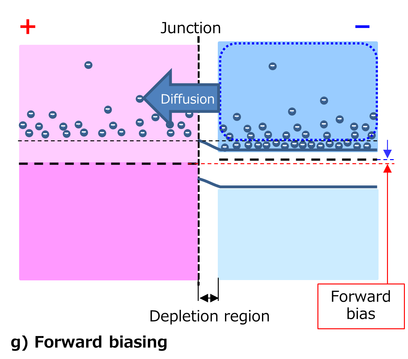
g) Forward-biased state
(i.e., when the metal is more positively biased than the n-type semiconductor)
The Fermi level of the n-type semiconductor increases by the amount of forward bias, causing the potential barrier to decrease. As a result, the number of electrons with energy greater than the potential barrier increases exponentially, causing diffusion current to flow. Only electrons contribute to this current since there is no hole in the metal. Therefore, an SBD is called a unipolar device. Since the potential barrier of the SBD is lower than that of the pn junction diode, current begins flowing in the SBD at a lower voltage than in the pn junction diode.
The depletion region that extends from the junction into the n-type semiconductor shrinks.
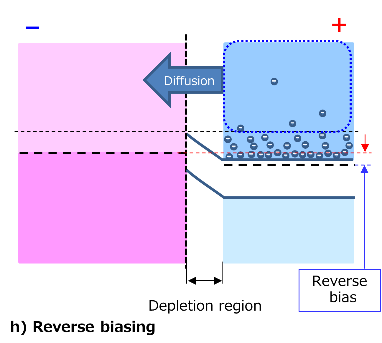
h) Reverse-biased state
(i.e., when n-type semiconductor is more positively biased than the metal)
The Fermi level of the n-type semiconductor decreases by the amount of reverse bias, causing the potential barrier to increase. As a result, the number of electrons with energy greater than the potential barrier decreases exponentially.
The depletion region that extends from the junction into the n-type semiconductor widens.
Related Links
For products, please refer to the following links.


