- General Top
- SEMICONDUCTOR
- STORAGE
- COMPANY
-
My ToshibaSemicon
- Semiconductor Top
-
ApplicationsAutomotive
Body Electronics
xEV
In-Vehicle Infotainment
Advanced Driver-Assistance Systems (ADAS)
Chassis
IndustrialInfrastructure
BEMS/HEMS
Factory Automation
Commercial Equipment
Consumer/PersonalIoT Equipment
Healthcare
Wearable Device
Mobile
Computer Peripherals
-
ProductsAutomotive Devices
Discrete Semiconductor
Diodes
Transistors
Logic ICs
Analog Devices
Digital Devices
Wireless Devices
※
 : Products list (parametric search)Power Semiconductors
SiC Power Devices
※
: Products list (parametric search)Isolators/Solid State RelaysPhotocouplers
Digital Isolators
Solid State Relays
Fiber Optic Transmitting Modules
※
: Products list (parametric search)MOSFETsIGBTs/IEGTsBipolar Transistors※
: Products list (parametric search)Diodes※
: Products list (parametric search)MicrocontrollersMotor Driver ICsIntelligent Power ICs※
: Products list (parametric search)Power Management ICsLinear ICs※
: Products list (parametric search)General Purpose Logic ICsLinear Image SensorsOther Product ICsOther Product ICs
※
: Products list (parametric search) -
Design & Development
-
Knowledge
- Where To Buy


- Part Number & Keyword Search
- Cross Reference Search
- Parametric Search
- Stock Check & Purchase
This webpage doesn't work with Internet Explorer. Please use the latest version of Google Chrome, Microsoft Edge, Mozilla Firefox or Safari.
require 3 characters or more. Search for multiple part numbers fromhere.
The information presented in this cross reference is based on TOSHIBA's selection criteria and should be treated as a suggestion only. Please carefully review the latest versions of all relevant information on the TOSHIBA products, including without limitation data sheets and validate all operating parameters of the TOSHIBA products to ensure that the suggested TOSHIBA products are truly compatible with your design and application.Please note that this cross reference is based on TOSHIBA's estimate of compatibility with other manufacturers' products, based on other manufacturers' published data, at the time the data was collected.TOSHIBA is not responsible for any incorrect or incomplete information. Information is subject to change at any time without notice.
require 3 characters or more.
How do ESD protection diodes operate?
ESD protection diodes are elements that turn on quickly with low impedance to protect ICs when high-voltage pulses such as those caused by electrostatic discharge (ESD) enter. We describe the behavior of the most commonly used ESD protection diodes for this application.
IoT devices, smartphones, and other mobile devices are ubiquitous now. As we plug and unplug USB, Lightning, and other cables to/from our electronic devices frequently, these electronic devices are becoming increasingly exposed to ESD strikes, making it more important than ever before to provide system-level ESD protection. ESD protection diodes are widely known as a solution for protection against static electricity. The following describes the operation of ESD protection diodes.
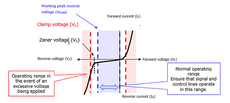
ESD protection diodes capitalize on the Zener breakdown* of pn junction diodes. As shown below, the pn junction diode conducts in the forward direction at approximately 0.7 V whereas it starts to conduct in the reverse direction at Zener voltage (VZ), which differs from diode to diode. ESD protection diodes capitalize on the reverse-bias characteristics of the pn junction.
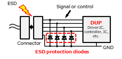
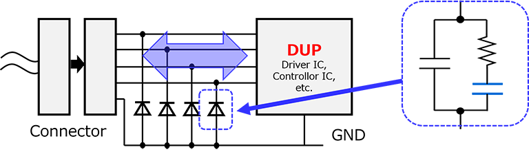
As shown in Figure 1, ESD protection diodes are connected along signal or control lines between a device under protection (DUP) and a connector that is exposed to ESD. In addition to Zener voltage (VZ), ESD protection diodes have a reverse-bias characteristic called working peak reverse voltage (VRWM). VZ is the minimum voltage at which an ESD protection diode turns on whereas VRWM is the maximum voltage at which it remains off. ESD protection diodes are always connected in reverse bias. Let VIN be the voltage of the signal line to which an ESD protection diode is connected. Then, it does not turn on when GND < VIN ≤ VRWM.
Suppose that an ESD surge enters a system while it is operating normally.
During normal operation, ESD protection diodes remain off.
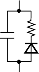
In this state, they act as capacitors with a total capacitance of CT because of the depletion region formed across the pn junction. CT differs from diode to diode and can be as low as 0.2 pF.
When ESD or other excessive voltage is applied, ESD protection diodes turn on.
At this time, ESD protection diodes can be regarded as consisting of a voltage source and a resistor with small dynamic resistance (RDYN). The voltage source provides forward voltage (VF) when it has forward bias with respect to a diode whereas it provides clamp voltage (VC), i.e., Zener voltage defined in the high-current region, when it has reverse bias with respect to a diode.

The ESD protection diodes act as capacitors in the off state and as a voltage source and tiny resistors in the on state. Also exercise care as to total capacitance when selecting ESD protection diodes for high-frequency lines.
Let us consider the tiny dynamic resistance (RDYN) of an ESD protection diode when it is on.
The following figure shows the simplest circuit configuration that represents how current flows through a circuit in the event of excessive voltage (e.g., an ESD surge).
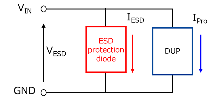
The ESD protection circuit is connected in parallel with a DUP as shown above. Therefore, the ESD surge voltage (VESD) that is applied across the ESD protection diode is also applied across the DUP. (In reality, the voltages applied to the ESD protection diode and the DUP and the application timing differ slightly because of the parasitic inductance and capacitance of board traces.) The current that flows to the DUP (IPro) is affected by the states of its internal active circuits and depends on VESD.
Therefore, the most important thing to protect the DUP is to reduce VESD, which depends on the clamp voltage of the ESD protection diode.
Figure 5 shows an equivalent circuit for an ESD protection diode in the on state, which indicates that there is dynamic resistance in series with the clamp voltage source. This means that as IESD increases, the resulting voltage drop is added to the clamp voltage.
ESD is a sudden discharge of static electricity that occurs when two electrically charged objects are brought into contact with each other. (For details, see the FAQ entry ”What is electrostatic discharge (ESD)?”).
What is electrostatic discharge (ESD)?
Just like the discharging of a capacitor, ESD exhibits extremely high current immediately after contact. For example, the peak current of the ESD waveform specified in IEC 61000-4-2, an ESD immunity test standard, is as high as 30 A. Suppose that an ESD protection diode has a dynamic resistance of 0.5 Ω. Then, the peak ESD current causes an instantaneous voltage drop of 15 V.
Therefore, in order to enhance the protection performance, it is important to select ESD protection diodes not only with low clamp voltage but also with low dynamic resistance, considering the resulting voltage drop.
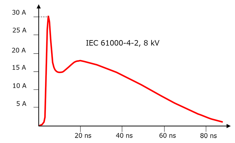
Figure 7 indicates that ESD is a high-frequency pulse that is applied instantaneously. Therefore, care should be taken as to the placement and the traces for ESD protection diodes in order to obtain the best performance from them.
For details, see the FAQ entry “Board design considerations for TVS diodes (ESD protection diodes).”
Board design considerations for TVS diodes (ESD protection diodes).
* When a silicon pn diode is reverse-biased, two types of breakdown occur: Zener breakdown and avalanche breakdown. There are no distinct mechanisms for these two types of breakdown. The pn junction is more likely to enter Zener breakdown at 5.6 V or lower voltage whereas avalanche breakdown is more dominant at higher voltage.
Related Links
For TVS diode (ESD protection diode) products, please refer to the following links.