
- General Top
- SEMICONDUCTOR
- STORAGE
- COMPANY
-
My ToshibaSemicon
- Semiconductor Top
-
ApplicationsAutomotive
Body Electronics
xEV
In-Vehicle Infotainment
Advanced Driver-Assistance Systems (ADAS)
Chassis
IndustrialInfrastructure
BEMS/HEMS
Factory Automation
Commercial Equipment
Consumer/PersonalIoT Equipment
Healthcare
Wearable Device
Mobile
Computer Peripherals
-
ProductsAutomotive Devices
Discrete Semiconductor
Diodes
Transistors
Logic ICs
Analog Devices
Digital Devices
Wireless Devices
※
 : Products list (parametric search)Power Semiconductors
SiC Power Devices
※
: Products list (parametric search)Isolators/Solid State RelaysPhotocouplers
Digital Isolators
Solid State Relays
Fiber Optic Transmitting Modules
※
: Products list (parametric search)MOSFETsIGBTs/IEGTsBipolar Transistors※
: Products list (parametric search)Diodes※
: Products list (parametric search)MicrocontrollersMotor Driver ICsIntelligent Power ICs※
: Products list (parametric search)Power Management ICsLinear ICs※
: Products list (parametric search)General Purpose Logic ICsLinear Image SensorsOther Product ICsOther Product ICs
※
: Products list (parametric search) -
Design & Development
-
Knowledge
- Where To Buy


- Part Number & Keyword Search
- Cross Reference Search
- Parametric Search
- Stock Check & Purchase
This webpage doesn't work with Internet Explorer. Please use the latest version of Google Chrome, Microsoft Edge, Mozilla Firefox or Safari.
require 3 characters or more. Search for multiple part numbers fromhere.
The information presented in this cross reference is based on TOSHIBA's selection criteria and should be treated as a suggestion only. Please carefully review the latest versions of all relevant information on the TOSHIBA products, including without limitation data sheets and validate all operating parameters of the TOSHIBA products to ensure that the suggested TOSHIBA products are truly compatible with your design and application.Please note that this cross reference is based on TOSHIBA's estimate of compatibility with other manufacturers' products, based on other manufacturers' published data, at the time the data was collected.TOSHIBA is not responsible for any incorrect or incomplete information. Information is subject to change at any time without notice.
require 3 characters or more.
What is the bootstrap circuit in high-voltage IPDs?
A bootstrap circuit is a circuit used to drive the gates of switching elements on the high side (upper arm) of full-bridge circuits, half-bridge circuits, etc. I The circuit comprises a diode and a bootstrap capacitor, which collectively produce the gate voltage necessary to operate the high-side component.
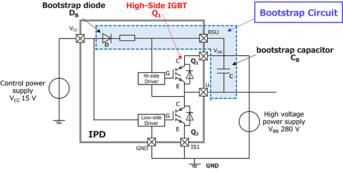
Fig. 1 shows a bootstrap circuit for one leg of a bridge circuit (one pair of high-side and low-side devices).
N-ch IGBTs (or MOSFETs) are driven by applying a voltage of about 10 to 15V to the gate-emitter (or gate-source). However, the emitter (or source) on the high-side side is not constant, and the voltage changes depending on the operation of the circuit. For example, when the high-side device is turned on, the potential difference between the collector and emitter becomes almost zero, and the emitter (or source) potential becomes the same potential as the high-voltage power supply (bridge line voltage). Also, when the high-side device is turned off and the switching device on the low-side (lower arm) is turned on, the emitter (or source) on the high-side becomes the GND potential.
To turn on the high-side IGBT, the potential difference between the gate and emitter must always be the gate-emitter drive voltage (10 to 15V). In other words, when the high-side element is on, the gate drive voltage required is the high-voltage power supply voltage plus the gate-emitter drive voltage (or gate-source drive voltage). This voltage is higher than the voltage applied externally and must be generated by the bootstrap circuit.
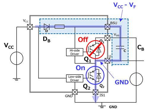
The operation of the IGBT-driven bootstrap circuit is explained below.
As shown in Fig. 2, when the high-side IGBT Q1 is off and the low-side IGBT Q2 is on, the emitter potential of Q1 drops to ground (GND). In this state, current flows from VCC → diode DB → bootstrap capacitor CB → Q2, charging CB.
The potential on the upper side of CB is charged to a value obtained by subtracting the forward voltage VF of diode DB from the control power supply voltage VCC. Meanwhile, the potential on the lower side of CB (the source potential of Q1) is GND because Q2 is on. Therefore, the voltage VCB across both ends of CB is VCB = VCC − VF.
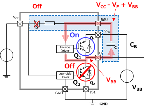
Thereafter, when Q2 turns off, the charging path for CB is cut off (DB is turned off), but because the charge on CB has not been discharged, the voltage VCB across both ends is maintained. At this point, Q1 is still off, and the emitter potential is GND. Next, when it is time to turn Q1 on, the charge stored in CB causes the voltage VCB to be applied to the gate. This gate-emitter potential difference VCB is sufficient to turn Q1 on, so Q1 becomes conductive.
As shown in Fig. 3, when Q1 turns on, its emitter potential becomes the same as the high-voltage power supply VBB. Even in this state, the charge of CB is maintained, and the voltage VCB across both ends is maintained. Since the potential on the lower side of CB is VBB, the potential on the upper side is VCB + VBB, which is a voltage that exceeds the high-voltage power supply voltage. Therefore, the potential difference between the gate and emitter of Q1 is maintained and is VCB, so Q1 remains on.
In this way, the bootstrap circuit generates the gate potential required to turn Q1 on, regardless of the emitter potential of Q1.
However, in order to charge the bootstrap capacitor CB, a period during which Q1 is off and Q2 is on is required. If this off time is too short, the voltage VCB across CB may not be charged sufficiently, and the gate drive voltage may be insufficient. This point requires careful consideration when designing the circuit.
Related Links
The following documents also contain related information.
Parametric Search
Intelligent Power ICs
FAQs
* Company names, product names, and service names used in this FAQ may be of their respective companies.