


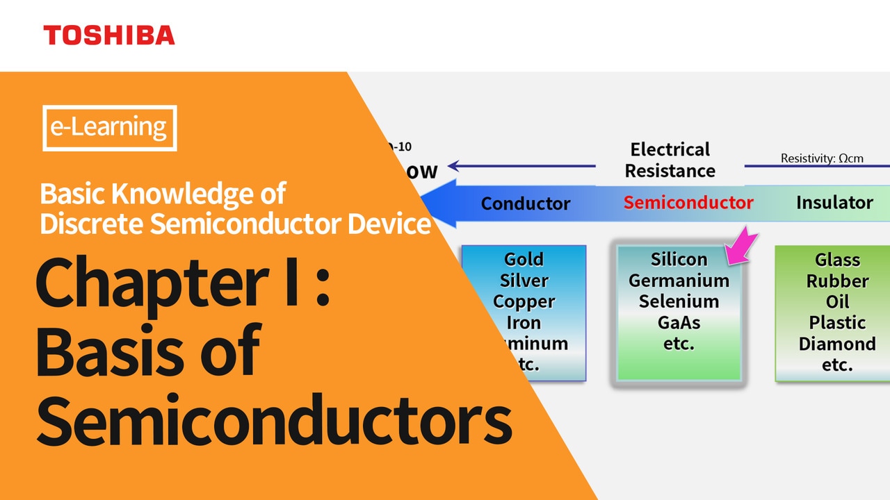
What types of structures are there in MOSFETs?
MOSFET structures can be broadly classified into the lateral structures and the vertical structures. They are categorized based on whether the current flows parallel to the surface (lateral direction) or perpendicular to the surface (vertical direction).
- Lateral structure features: Source and drain are on the same plane, current flows horizontally, simple structure suitable for ICs.
- Vertical structure features: Source at the top, the drain at the bottom, current flows vertically, supports high voltage and large current.
Here, we focus on the mainstream N-channel MOSFET. In an N-channel MOSFET, two n-type regions that serve as the source and drain are formed within a p-type substrate (called the body). Above these regions, a gate electrode is placed, separated by a thin oxide layer, and the gate is electrically insulated from the source and the drain. Each region has its own electrode: the two n-type regions are connected to the source (S) and drain (D), while the electrode placed on the oxide layer is called the gate (G). The body terminal is usually connected to the source electrode (the lowest potential).
When a gate voltage is applied, the potential difference between the gate and the body creates an inversion layer on the surface of the substrate. This inversion layer forms a conduction path (called the channel) from the source to the drain. Furthermore, when a drain-source voltage (VDS) is applied, a potential gradient appears along the channel, and the drain side becomes higher in potential than the source. As this potential difference increases, the drain-side portion of the channel undergoes pinch-off and the channel is interrupted. A depletion region then expands near the drain, and carriers drift through this region under the influence of the electric field to reach the drain. This is known as the saturation operation (or the saturation region) of the MOSFET.
For more details on saturation, please refer to the FAQ: MOSFET Operation.
The basic structures of lateral and vertical types are shown in Figure 1.
Lateral structure: All three terminals (drain, source, gate) are located on the top surface. The bottom surface is a terminal called the body (B), which is usually connected to the source. The drain current flows horizontally from the drain to the source. As all terminals are on the top and the structure is simple, it is easy to make into an IC, and is often used in ICs and LSIs such as CMOS logic ICs. In addition, because of their low capacitance, horizontal MOSFETs are used in RF amplifiers, etc.
Vertical structure: Two terminals (source and gate) are placed on the top surface, and the drain is placed on the back surface. The layer (P-body) equivalent to the body of a lateral MOSFET is connected to the source electrode on the top surface. The drain current flows vertically from the drain to the source. This structure allows for high voltage resistance, and most medium and high voltage MOSFETs have this structure.
The planar gate structure is a general-purpose lateral structure process. In vertical structures, trench gate structures and super-junction (SJ) structures, which have significantly improved characteristics, are the mainstream. Recently, field plate (FP) structures that apply the RESURF (Reduced Surface Field) principle have been developed.
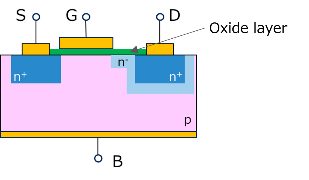
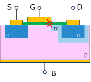
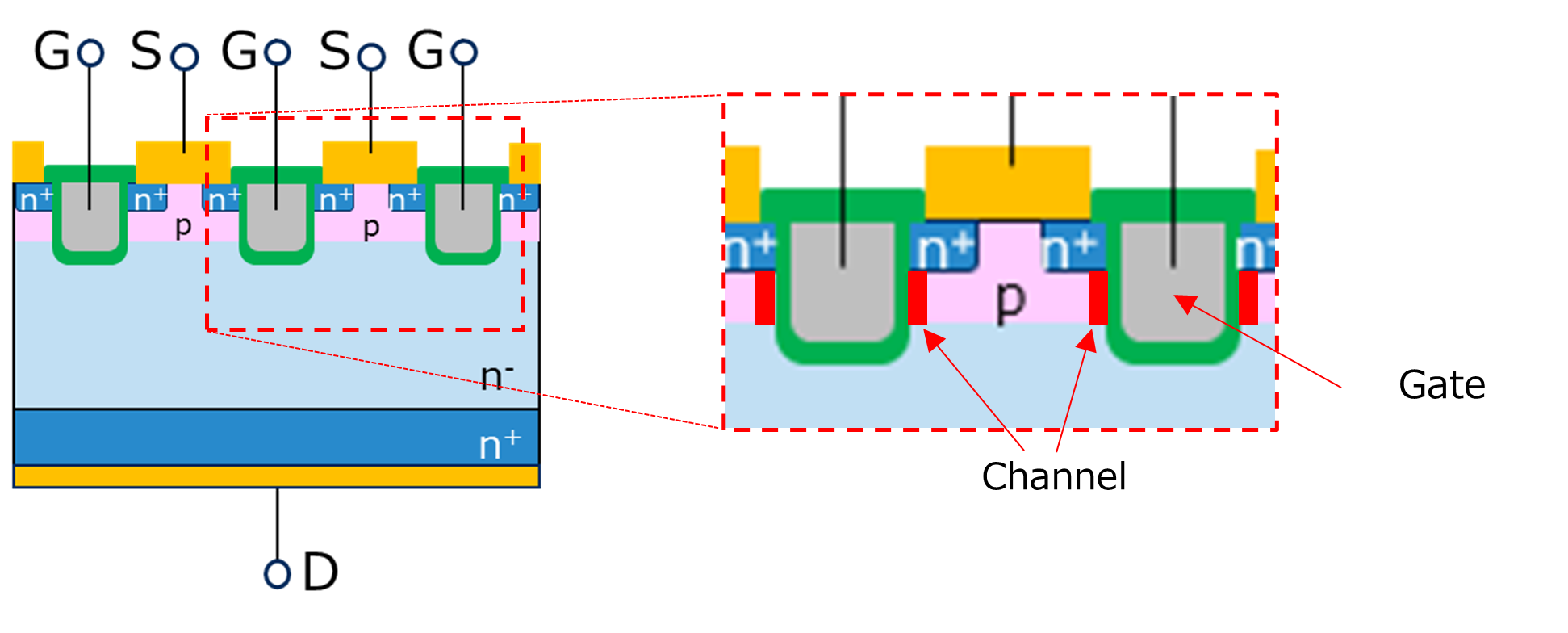
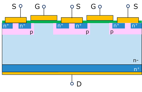
a) Lateral structure
Terminals for Source (S), Gate (G), and Drain (D) are located on the top surface, and the Body (B) terminal is on the backside. The n+ region on the drain side is surrounded by an n− layer, which extends slightly toward the source under the gate to maintain breakdown voltage.
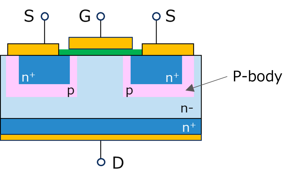
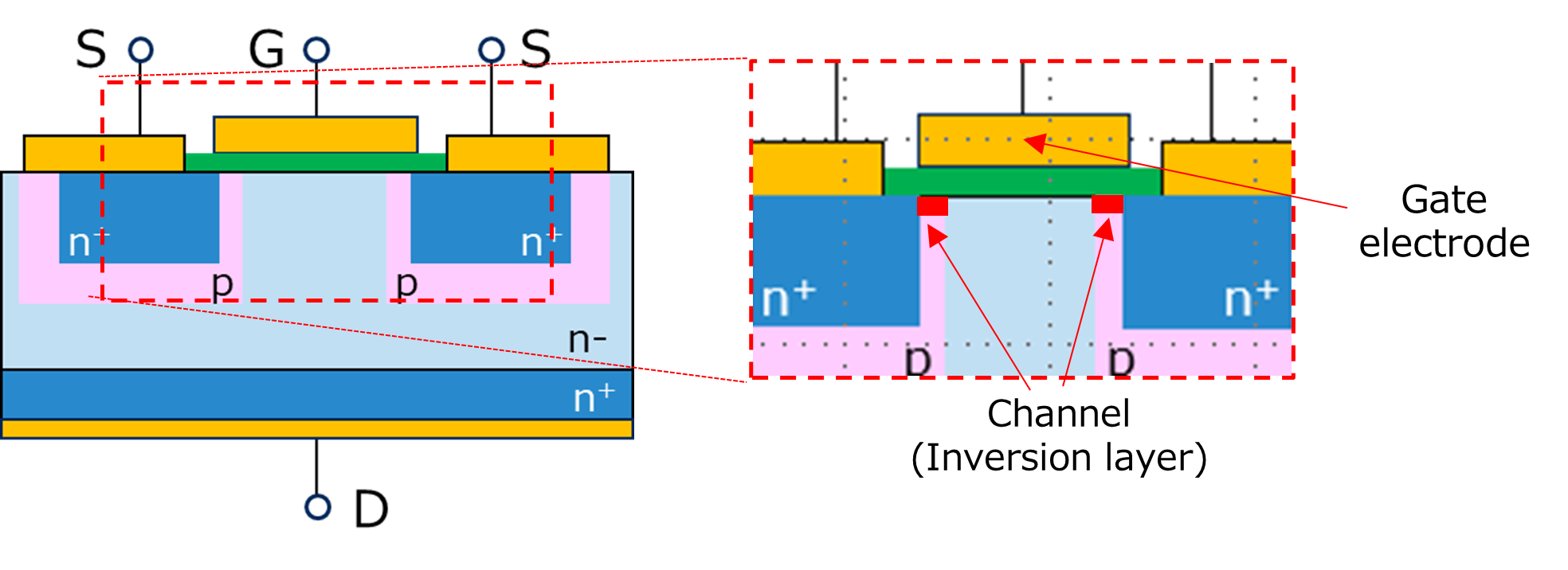
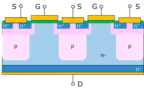
b) Vertical structure
Terminals for Source (S) and Gate (G) are on the top surface, and the Drain (D) terminal is on the backside. The n+ source region is surrounded by a p-type layer, which is referred to as the p-body.
Figure 1 N-ch MOSFET structure (vertical and lateral)
This figure shows simplified cross-sectional diagrams of N-channel MOSFET structures.
The features of MOSFETs with each structure are as follows:
Lateral structure
- The process is simple and the gate, drain, and source terminals are all on the top surface, so it is often used as an IC process.
- Small gate-drain capacitance CGD, suitable for high-speed applications.
- Difficult to form high voltage and high current elements (VDSS < 100 to 200V at practical level).
Vertical structure
- The drain is on the back surface, so it must be drawn to the top surface for IC integration.
- Gate-drain capacitance CGD is large.
- Low on-resistance is easily achieved because the current on the drain side is widely diffused toward the back surface.
- Relatively easy to increase MOSFET breakdown voltage (VDSS).
Higher breakdown voltage of MOSFET
The breakdown voltage between the drain and source of a MOSFET can be increased by lowering the impurity concentration in the n-drift layer (drain). However, lowering this impurity concentration increases the breakdown voltage, but at the same time increases the on-resistance.
Lateral structure: The breakdown voltage between the drain and source of a MOSFET can be increased by lowering the impurity concentration in the n-drift layer (drain). However, lowering this impurity concentration increases the breakdown voltage, but at the same time increases the on-resistance.
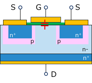
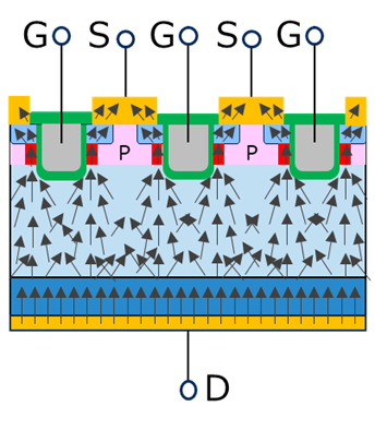
Vertical structure: The back surface is the drain electrode. ID flows from this wide drain toward the inversion layer (yellow line in Figure 2 b). As with the lateral type, a high breakdown voltage can be achieved by lowering the concentration of the n-layer. Unlike the lateral type, current flows widely through the n-layer, which acts as a resistor, so a low on-resistance (≒ high current) can be achieved in a smaller area than the lateral type. Similarly, for the same on-resistance, the vertical type can achieve a high breakdown voltage VDSS.
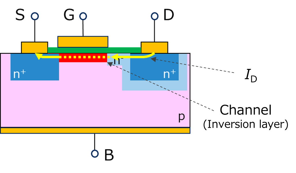
a) Lateral structure
Current flows laterally from the drain to the source. It travels from the n+ drain region through the n- layer and the inversion layer (channel) directly below the gate to the source.
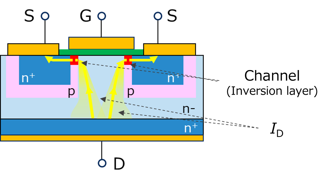
b) Vertical structure
Current flows vertically from the drain to the source. The current passes from the drain on the backside through the n-layer, and then reaches the source via the inversion layer formed just below the gate oxide of the p-body that is in contact with the gate oxide.
Figure-2 N-ch MOSFET current path when on state
Input capacitance and feedback capacitance of MOSFET
Vertical MOSFETs have larger input capacitance Ciss and feedback capacitance Crss than lateral MOSFETs.
The biggest difference between vertical and lateral types is the capacitance between the gate and drain, as shown in Figure 3. In the lateral type, the part facing the gate electrode is the p-layer of the body. Therefore, the part where the gate faces the drain is very small. In contrast, in the vertical type, the part facing the gate electrode is the n-layer of the drain. For this reason, the vertical type has a larger CGD than the lateral type.
If the gate-source capacitance is CGS, the gate-drain capacitance is CGD, and the drain-source capacitance is CDS, the input capacitance Ciss, feedback capacitance Crss, and output capacitance Coss used in circuit design are expressed by the following formulas.
- Ciss = CGS + CGD
- Coss = CDS + CGD
- Crss = CGD
For this reason, the vertical type has larger Ciss, Coss, and Crss than the lateral type.
a) Lateral structure
In a lateral MOSFET, the capacitance is formed between the gate and the n⁻ region near the drain. Because the opposing area is small, CGD remains low.
b) Vertical structure
In a vertical MOSFET, the gate faces a wide n⁻ region, resulting in a much larger gate-to-drain capacitance (CGD).
Figure 3 N-ch MOSFET Gate-drain capacitance CGD
This figure uses the structure diagram from Figure 1 to show where the gate-to-drain capacitance (CGD) occurs in lateral and vertical MOSFETs.
Against this background, lateral type MOSFETs are used for the output of wireless communication devices (RF amplifiers), and vertical type MOSFETs are used in power supply circuits such as switching power supplies, DC-DC converters, and load switches. For vertical structures, further process improvements are being made to improve performance. One of the purposes of these process improvements is to reduce on-resistance.
On-resistance
The on-resistance (RDS(ON)) of a MOSFET is explained below.
The drain-source breakdown voltage VDSS and on-resistance RDS(ON) of a MOSFET have a relationship where RDS(ON) increases as VDSS increases. Furthermore, resistance R is expressed as follows using the cross-sectional area S, length l, and resistivity ρ.
R = ρ x l / S
Therefore, the resistance value will be smaller if the length l is shorter, the cross-sectional area S is wider, and the resistivity ρ is lower. In the case of semiconductors, resistivity is expressed by the following formula, where N is the impurity concentration, μ is the mobility, and q is the electron charge.
ρ = 1 / ( q x μ x N )
To reduce resistivity (ρ), increasing N (carrier concentration), μ (mobility), or q (elementary charge) would be effective. However, q is a physical constant, and μ is strongly dependent on the material and physical properties, so it is not easy to freely increase it in the process. Therefore, it is understood that the only way to lower resistivity through processing is by increasing the carrier concentration N.
When a reverse bias VDSS is applied to the drain and source when the MOSFET is off, the depletion layer extends in proportion to this reverse bias. Also, the lower the impurity concentration N, the farther the depletion layer extends. It is considered that there are no majority carriers in the depletion layer, and only impurity ions (fixed charges) exist. When the combined electric field caused by this fixed charge exceeds the critical electric field Ecritical, avalanche breakdown occurs. The maximum voltage at which this avalanche breakdown does not occur is the breakdown voltage VDSS. In this way, increasing N decreases R, but at the same time VDSS also decreases, and decreasing N increases R, but VDSS increases. This trade-off relationship mainly depends on the impurity concentration N.
In an N-ch MOSFET, when an on-voltage is applied between the gate and source, an inversion layer forms in the p-layer directly below the gate. Although this inversion layer is a p-layer, it has an excess of electrons, similar to an n-layer. This inversion layer (also called a channel) connects the drain and source, turning the MOSFET on. The on-state has a linear region and a saturation region, and here we will explain the on-resistance in the linear region. For an explanation of MOSFET operation, including the saturation region, please refer to the following FAQ.
What is the operation of a MOSFET?
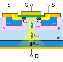
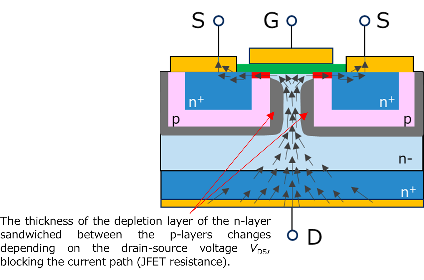
The path of current flowing from drain to source is shown in Figure 4a. The cause of resistance varies depending on the region through which this current flows. These are divided into resistances shown in Figure 4b. We will briefly explain each resistance.
- Channel resistance RCH: The resistance of the channel region, which varies depending on the width and length of the channel and the mobility and density of carriers.
- JFET resistance RJFET: The thickness of the depletion layer in the pn junction between the p-type regions changes with the drain-to-source voltage (VDS). This variation alters the width of the current path, which in turn changes the resistance value. Because this behavior resembles that of a JFET, it is called JFET resistance.
Notably, JFET resistance is characteristic of vertical MOSFETs, where it occurs due to the narrowing of the current path caused by the depletion layer between the p-type regions near the source. - Drift resistance Rdrift: Resistance due to the n- layer from the P region to the n+ region, which is the substrate. In high-voltage MOSFETs, the n- layer determines the withstand voltage, and the higher the withstand voltage, the lower the concentration and the higher the resistance.
- Substrate resistance Rsub: Resistance of the substrate region. It varies depending on the concentration and depth of the n- layer, and the path that the current flows and how it spreads.
As mentioned earlier, there is a trade-off between RDS(ON) and VDSS. Therefore, the ratio of these resistances to the on-resistance (RDS(ON)) will differ between a MOSFET with VDSS = 40V and a MOSFET with VDSS = 600V. In particular, the proportion of the drift region resistance Rdrift, which mainly affects VDSS, becomes larger in higher voltage MOSFETs.
For the same planar gate type MOSFET, this proportion is as follows (although the figures are not precise as they vary depending on the product):
40V :RCH = 10%、RJFET = 40%、Rdrift=40%、Rsub =10%
600V :RCH = 1%、RJFET = 20%、 Rdrift=80%、Rsub =0%
Therefore, the method for reducing on-resistance differs depending on the target voltage.
- Low-voltage MOSFET: Reduce channel resistance and JFET resistance → Trench gate structure
- High-voltage MOSFET: Reduce drift resistance → Super-junction structure
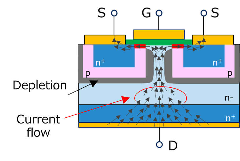
a) Current flow
In the ON state, current flows from the center of the drain on the backside toward the region between the sources.
b) On-resistance RDS(ON)
The on-resistance consists of channel resistance (RCH), JFET resistance (RJFET), drift resistance (Rdrift), and substrate resistance (Rsub). Each component arises from the structure and position of the current path.
Figure 4 Vertical N-ch MOSFET Current flow and on-resistance
This figure illustrates the current path during the ON state and the components that make up the on-resistance in a vertical N-channel MOSFET.
Trench gate structure
The biggest difference from the conventional planar gate structure is the gate arrangement. In conventional planar gate structures, the gate electrode is placed on the surface of the device, but in trench gate structures, a groove is dug from the surface of the device and the gate electrode is embedded in it. (Figure 5 Trench gate structure and planar gate structure) The inversion layer is formed vertically instead of horizontally as in conventional structures. This has the following advantages.
- Miniaturization is possible, allowing the number of channels per unit area to be increased, significantly reducing the channel resistance.
- The structure eliminates the JFET that blocks the current path, so JFET resistance is significantly reduced.
- The current density is higher than in planar structures, allowing more current to flow in a chip of the same area (Figure 6).
- Gate charge tends to decrease, although it depends on the process design.
a) Trench Gate Structure
A simplified cross-sectional view of the trench structure.
The inversion layer is formed vertically along the gate, which increases channel density and reduces channel resistance. This design also minimizes the impact of JFET resistance.
b) Planar Gate Structure
The conventional vertical MOSFET structure. The inversion layer is formed horizontally along the surface, making the current path narrower and causing a significant influence from JFET resistance.
Figure 5 Trench gate structure and planar gate structure (N-ch MOSFET )
This figure compares the trench gate structure and the planar gate structure in N-channel MOSFETs.
The most significant difference is the orientation of the inversion layer: planar structures form it horizontally along the surface, while trench structures form it vertically along the gate.
a) Trench Gate Structure
Current path in a planar structure. In a planar structure, the current path is narrow and the JFET resistance is high.
b) Planar Gate Structure
Current flows through a narrow horizontal path, making the effect of JFET resistance significant.
Figure 6 Current flow in trench gate structure and planar gate structure
This figure compares the current paths in trench and planar MOSFET structures, highlighting the influence of JFET resistance.
Super-junction structure
In order to increase the breakdown voltage of MOSFETs, it is necessary to lower the concentration of the drift region (n-layer) and at the same time increase the thickness of the n-layer. However, this causes the problem of increasing the drift resistance that constitutes the on-resistance of the MOSFET. The super-junction structure is used as a solution to this problem.
Since the conventional planar structure is a flat structure, the electric field is strongest at the interface between the n layer (n-layer) and the p layer. In contrast, the super-junction structure is a structure in which a p layer (P pillar layer) is formed in a columnar shape in part of the n-layer, and P-N layers are arranged alternately. Therefore, the interface between the n layer (n-layer) and the p layer exists in the vertical direction (depth direction). The depletion layer spreads along this pn junction, and when a high voltage is applied, this columnar part becomes completely depleted.
The electric field strength is highest at the interface as in the conventional structure, but the electric field is distributed and uniformed in the vertical direction (along the columnar shape). This makes it possible to apply a higher voltage (drain-source voltage VDS) between the drain and source than in the conventional structure with the same impurity concentration. This means that for the same withstand voltage (VDSS), it is possible to achieve a MOSFET with a lower on-resistance (RDS(ON)).
a) Planar gate structure
A conventional vertical structure where the n-type and p-type boundary is planar. To achieve high breakdown voltage, the drift layer (n⁻ layer) must have low impurity concentration and increased thickness.
b) Super-junction structure
P-type columns are formed within the n-type layer, with alternating P-N layers. Under high voltage, the columnar regions become fully depleted, resulting in a uniform electric field.
Figure 7 Super-junction structure and planar gate structure
This figure compares MOSFET structures designed to achieve high breakdown voltage. In the superjunction structure, p-type layers (P-pillars) are formed as columns within the n-type layer, and P-N layers are alternately arranged vertically. This design helps distribute the electric field laterally, enabling both high breakdown voltage and low on-resistance.
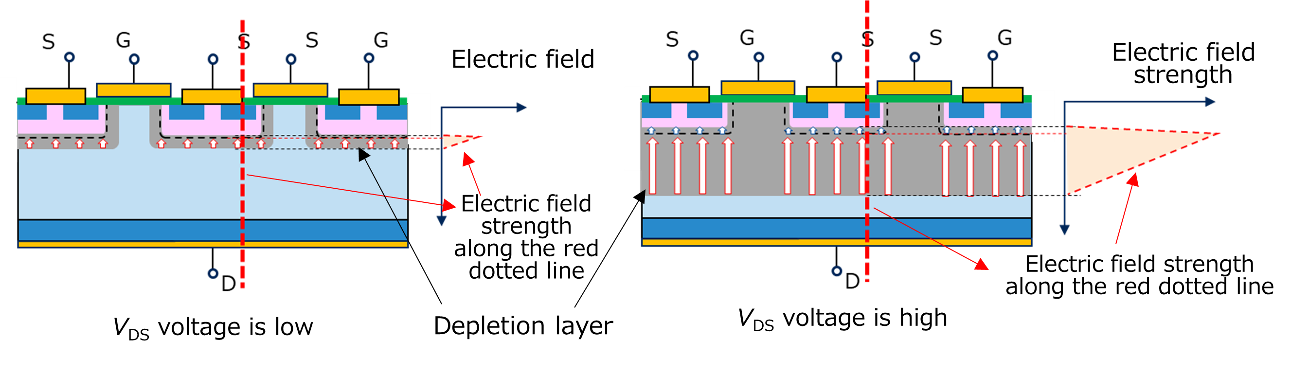
a) Planar gate structure
· Low VDS: The depletion region partially extends into the drift layer (n⁻ layer), and the electric field concentrates near the p-n junction.
· High VDS: The drift layer becomes fully depleted, but the electric field still tends to concentrate at the boundary, limiting performance under high voltage.
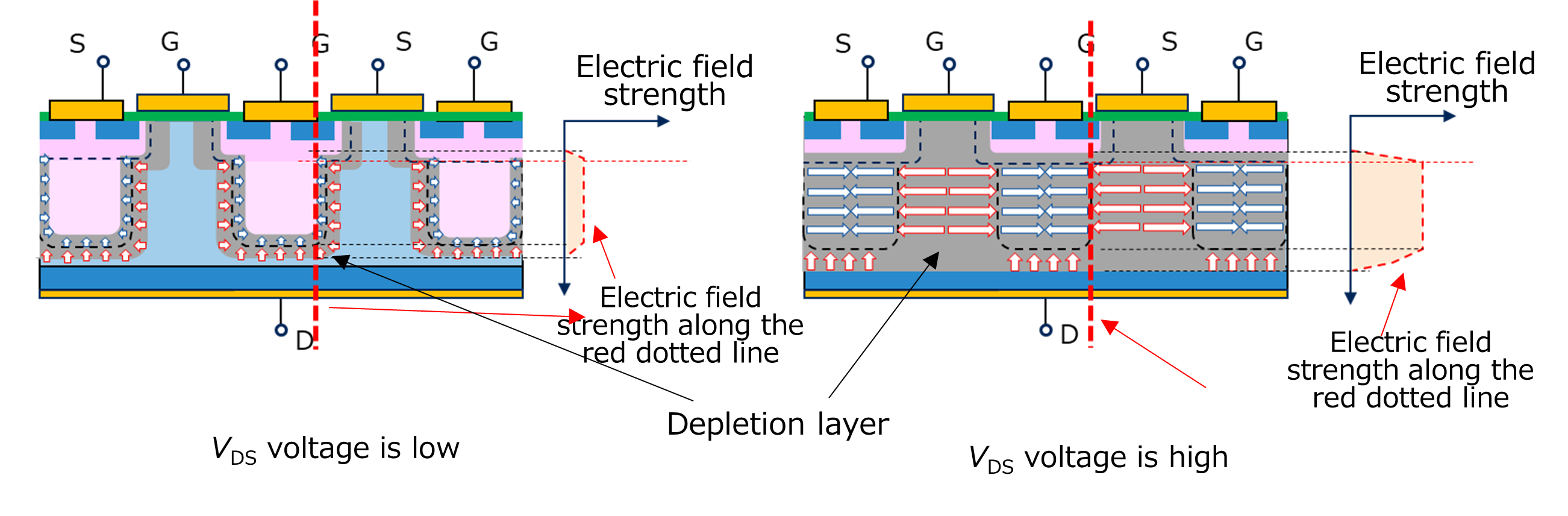
b) Super-junction structure
· Low VDS: The depletion region has not fully extended, and the electric field is locally distributed.
· High VDS: The alternating P-N layers become fully depleted, and the electric field is laterally distributed and uniform. This reduces field concentration and enables high breakdown voltage.
Figure 8 Electric field conditions when the MOSFET is off in the super-junction structure and the planar gate structure.
This figure compares the electric field distribution when the drain-source voltage (VDS) is low (before full depletion) and high (after full depletion) in the OFF state. The diagrams show the spread of the depletion region, and the electric field strength along the red dotted line—from the source through the n⁻ layer, p layer, and n layer—is illustrated on the right side of each diagram.
Related Links
Please refer to the following pages and documents for product lineup and other documents.
Parametric Search
MOSFETs
FAQs
Others

Online Circuit Simulator
The Online Circuit Simulator allows users to verify and select MOSFETs. (Members only)
* Company names, product names, and service names used in this FAQ may be of their respective companies.