


Understanding MOSFET Operation Principles and Mechanisms | Cutoff, Linear, and Saturation Regions Explained
What is MOSFET Operation?
MOSFETs are widely used semiconductor devices in electronic circuits. This FAQ explains MOSFET operating regions (cutoff, linear, and saturation), the meaning of threshold voltage and pinch-off voltage, and the mechanism of turning on and off in a way that beginners can easily understand.
In particular, understanding the saturation region is closely related to the operation of the MOS capacitor, and we will explain this mechanism in detail. We will also touch on the differences between lateral and vertical structures.
Note on Threshold Voltage (Vth)
In this FAQ, Vth refers to the MOSFET gate threshold voltage—the gate-to-source voltage at which an inversion layer forms and the MOSFET turns on. This is different from the thermal voltage (approximately 26 mV) commonly mentioned in BJT theory.
Overview of MOSFET
A MOSFET has three terminals: drain, source, and gate, and its on/off state is controlled by the voltage between the gate and source.
There are three operating regions: the cutoff region (off state), and two on states—the linear region and the saturation region.
When the gate-to-source voltage exceeds the threshold voltage (Vth), an inversion layer forms beneath the gate, turning the MOSFET on. If the drain-to-source voltage is lower than the pinch-off voltage (VP), the MOSFET operates in the linear region; if higher, part of the inversion layer becomes a depletion region, and the MOSFET operates in the saturation region. In saturation, the drain current remains almost constant regardless of VDS.
To understand this in more detail, knowledge of the MOS capacitor is necessary.
MOSFETs have lateral and vertical structures, but here we focus on the lateral structure. For differences between lateral and vertical types, see FAQ: MOSFET structure.
MOSFET Operating Region
MOSFETs have the following three operating regions. These ranges are shown on the ID-VDS curve in Figure 1, which is known as the static characteristics of MOSFETs.
- Cutoff region:
Even if the drain-source voltage VDS is increased, the drain current ID does not flow. - Linear region:
ID flows in proportion to VDS. - Saturation region:
ID is not proportional to VDS. An almost constant ID flows that depends on the gate-source voltage.
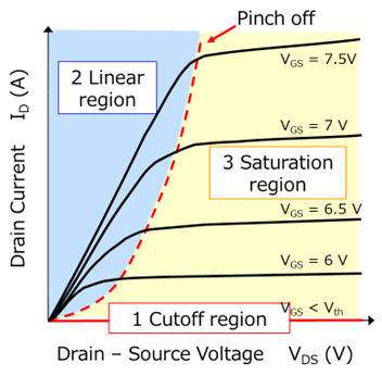
Figure 1 : MOSFET static characteristics (ID- VDS curve)
This graph shows the MOSFET VDS-ID characteristics, illustrating the three operating regions: cutoff, linear, and saturation. The pinch-off voltage marking the boundary between the linear and saturation regions is also indicated.
MOSFET On/Off Conditions (Threshold and Pinch-Off Voltage)
In the circuit shown in Figure 2, when VDS is applied between the drain and source and the voltage between the gate and source is gradually increased, the MOSFET turns on. The voltage at which it turns on is called the gate threshold voltage Vth.
The on-state is divided into the linear region and the saturation region depending on the applied VDS voltage (see Fig. 1).
- Off Condition:
VGS < Vth → MOSFET is off (cutoff region). - On Condition:
VGS ≥ Vth → MOSFET is on.
・0 < VDS ≦ VGS – Vth → MOSFET operates in the linear region.
・VDS ≧ VGS – Vth → MOSFET operates in the saturation region.
The boundary voltage is called the pinch-off voltage VP (VP = VGS - Vth).
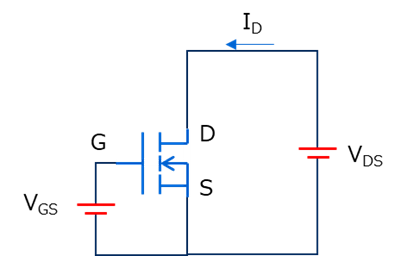
Figure 2 : VDS-ID measurement circuit
Basic circuit for measuring MOSFET VDS-ID characteristics. VDS is applied between drain and source, and VGS between gate and source to observe operating regions.
Important: Vth in this section refers to the MOSFET gate threshold voltage. Do not confuse this with the thermal voltage used in BJT calculations—they are completely different concepts.
MOSFET Physical Structure and Back Gate
Below is a brief explanation of the physical behavior.
The simplest lateral N-ch MOSFET consists of a p-type substrate, two n-type regions embedded in the p-type substrate,
and a metal plate that covers these two n-type regions and is insulated from the semiconductor, as shown in Figure 3. This metal plate, insulating film, and p-type substrate function as a MOS capacitor.
Each region has an electrode, and the two terminals of the n-type region are called the source (S) and drain (D), and the terminal of the MOS capacitor is called the gate (G). The back terminal is called the backgate (or body), and in discrete elements, it is usually connected to the source inside the package. Therefore, it is rarely taken into consideration when using MOSFETs.
The backgate is a terminal that is connected to the substrate (well, bulk) that constitutes the MOSFET. This terminal is supposed to be connected to a potential below the minimum potential applied to the MOSFET in the case of an N-ch MOSFET, and to a potential above the maximum potential in the case of a P-ch MOSFET. If this terminal does not meet this condition, for example, in the case of an N-ch MOSFET, the pn junction between the source terminal (S) and the backgate (B) will be turned on, and the MOSFET will not operate as a MOSFET, that is, it will not turn on or off due to the gate voltage. In general applications, the source terminal is used at the lowest potential in an N-ch MOSFET and at the highest potential in a P-ch MOSFET. For this reason, discrete elements are packaged with the source and backgate shorted internally.
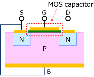
Figure 3 : Simplified cross-sectional view of a lateral type N-ch MOSFET
Basic structure of a MOSFET showing four terminals: drain (D), source (S), gate (G), and body/back gate (B). The MOS capacitor is located between the gate electrode and the p-type substrate across the insulating layer.
Operation of an N-ch MOSFET
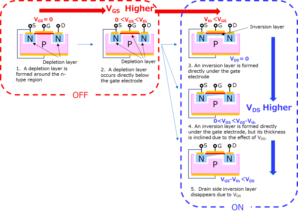
Figure 4 : Operation of lateral type N-ch MOSFET
Changes in MOSFET operating states. As VGS increases, the diagram shows the transition from no bias to depletion and inversion layer formation, followed by applying VDS to illustrate the linear region (continuous inversion layer) and saturation region (inversion layer pinched off near the drain).
In a MOSFET, a channel layer (inversion layer) is formed between the drain and source due to the potential difference between the gate and source, and the MOSFET turns on. The on and off states are explained using Figure 4.
- No bias state: VGS = 0: A depletion layer is formed between the buried n-type region and the p-type substrate.
- Depletion state: VGS < Vth: When a positive voltage is applied to the gate, the electrode side becomes positively charged and the semiconductor side becomes negatively charged, which offsets the holes in the P-type semiconductor and creates a depletion layer directly below the gate.
These two states are the off state of a MOSFET. - Inversion state: VGS ≧ Vth: If the gate voltage increases further, electrons gather directly below the gate electrode and an inversion layer is formed.
This creates a state similar to that of an n-type semiconductor, and the source and gate are connected by this inversion layer. In the case of an N-ch MOSFET, the inversion layer is in a state where there is an excess of free electrons, so it has the same properties as an n-type semiconductor. The drain and source are connected by this inversion layer This inversion layer forms a channel between the drain and source through which current can flow.
This inversion state is called the on-state of the MOSFET. The on-state of a MOSFET can be in two states: the linear region and the saturation region, as shown in Figure 1. Each state is determined by the voltage VDS applied between the drain and source. - On in the linear region 0 < VDS ≦ VGS – Vth : The inversion layer becomes shallower closer to the drain, but it is formed continuously between the drain and source. Therefore, ID flows in a manner nearly proportional to VDS.
- On in the saturation region VDS ≧ VGS – Vth : The inversion layer is discontinued near the drain. The drain current (electrons injected from the source) flows through the depletion layer between the inversion layer and the drain. However, the drain current is almost constant when VGS is fixed.
MOS Capacitor
To gain a deeper understanding, it is important to understand MOS capacitors.
The MOS capacitor is the area enclosed by the dotted line in Figure 3. Figure 5 shows the MOS capacitor and energy band states for states 1 to 3 described in Figure 4. The MOS capacitor is rotated 90° to the left to match the energy band diagram.
The MOS capacitor of an N-channel MOSFET consists of a metal electrode and a p-type substrate sandwiched between an insulating film. This MOS capacitor's state changes depending on the voltage between the electrode (G), which corresponds to the gate of the MOSFET, and the back gate (B). Since the back gate and source are short-circuited and have the same potential, we use the VGS parameter commonly used for MOSFETs.
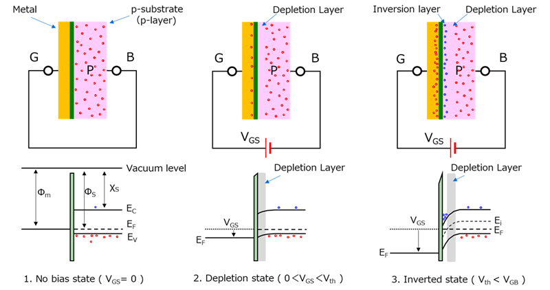
Figure 5 : MOS capacitance and energy band diagram
Structure of the MOS capacitor and its three operating states. The top row shows cross-sectional views of the MOS capacitor (metal electrode, insulating layer, p-type substrate) under no bias, bias below threshold voltage, and bias above threshold voltage. The bottom row illustrates the corresponding energy band diagrams, indicating flat-band, depletion, and inversion states.
- No bias state:
The energy state is as shown in the figure. In this state, nothing is generated directly below the insulating film. In this example, the work function Φm of the metal and the work function ΦS of the p-type semiconductor (the difference between the Fermi level and the vacuum level) are considered identical, resulting in no band bending (flat band state). However, they are usually different, which causes band bending. The difference in work functions (ΦS - Φm) is called the flat band voltage. - Depletion state:
A voltage of 0<VGS<Vth is applied, causing band bending. The applied voltage causes the impurities (such as B) that make up the p-type to capture electrons, forming a depletion layer only on the p-type semiconductor side. (The reason the gate side drops even though a positive voltage is applied to the gate side is because the energy band diagram is based on electrons.) - Inversion state:
When Vth<VGS is applied, the band bends further. Near the insulating film, this bending causes the Fermi level EF to become higher than the intrinsic Fermi level Ei, resulting in inversion from p-type to n-type. Electrons, which are p-type minority carriers, accumulate in this area.
In this way, the state of the MOS capacitance changes depending on the voltage VGS applied between the electrode (G) and backgate (B). The MOSFET is turned on and off by switching between the inversion state and other states.
However, another state occurs due to the voltage applied between the drain and source, which is not considered here. This is saturation.
MOSFET Saturation
MOSFET has two on-states: the linear region and the saturation region (see Fig. 1). When the gate voltage VGS exceeds the threshold voltage Vth and the MOSFET turns on, as the drain voltage VDS increases, the inversion layer (channel) near the drain becomes depleted and the inversion layer is cut off. The voltage at this boundary is called the pinch-off voltage VP, expressed as VP = VGS - Vth. The condition for saturation is VDS ≥ VGS - Vth.
When entering the saturation state, even if VDS is increased, the drain current ID becomes almost constant. The reason why it becomes constant is explained below.
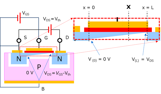
When VGS > Vth and VDS = 0V, the potential difference between the gate and the p-type semiconductor is the same near the source and near the drain, and a uniform inversion layer is formed (see Fig. 6).
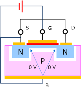
Figure 6 : N-ch MOSFET in inversion state
(VDS = 0、VGS > Vth)
A uniform inversion layer is formed by the gate voltage, and the drain and source are connected.
When VGS > Vth and a voltage VDS is applied between the drain and source, the source side is 0V and the drain side is VDS. When VDS is applied, the potential in the inversion layer changes continuously from the source to the drain (see Fig. 7).
Figure 7 : N-ch MOSFET in inversion state
(VDS=VGS-Vth、VGS>Vth)
The inversion layer is thick near the source and thin near the drain, showing the state just before pinch-off.
If the distance from the source to the drain is L, the potential at position x is V(x), and the potential difference between the gate and the substrate at that position is expressed as:
VGS(x)=VGS–V(x)
If this potential difference is greater than Vth, the inversion layer is formed; if less, only a depletion region exists.
- If VGS – V(x) ≥ Vth, an inversion layer is formed.
- If VGS − V(x) < Vth (for positions from x to L), only a depletion region exists.
The case where VGS − V(x’) = Vth occurs is shown in Fig. 8.
Figure 8 : N-ch MOSFET in inversion state
(V(x')=VGS –Vth、VGS>Vth)
Fig. 8 shows the saturation state of N-ch MOSFET (VGS > Vth, VGS − VDS < Vth). The pinch-off point is indicated, and the back gate reference potential to each point from source to drain is displayed.
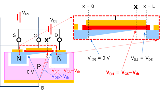
The position where VGS − V(x’) = Vth is called the pinch-off point. From the pinch-off point to the drain end, the region becomes a depletion layer. Although the depletion layer contains almost no carriers, as shown in the energy band diagram in Fig. 9, there is no diffusion barrier from source to drain. Therefore, electrons are accelerated by the electric field through the depletion layer and reach the drain.
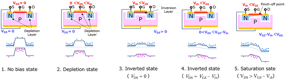
Figure 9 : Energy band diagram between source and drain
Fig. 9 shows the energy band diagrams of MOSFET for each state. In the saturation state, there is no barrier beyond the pinch-off point, and electrons are accelerated by the electric field.
Therefore, the drain current is determined by the voltage applied to the inversion layer up to this x’ (VGS − Vth) and the channel resistance of that section. If this resistance is Rch(sat), the drain current in saturation is expressed as:
ID(sat) = (VGS − Vth) / Rch(sat)
For this reason, in the saturation state, the drain current hardly depends on VDS. However, as VDS increases, the pinch-off point moves toward the source, the channel length becomes shorter, Rch(sat) decreases, and ID slightly increases (channel length modulation effect). Fig. 10 shows the increase state in actual products.
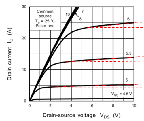
Figure 10 : N-ch MOSFET ID-VDS curve (TK155A60Z1)
Fig. 10 shows the ID-VDS curve of N-ch MOSFET (TK155A60Z1). In the saturation region, the current is ideally constant, but in reality, it slightly increases as VDS increases. The red dotted line indicates the ideal constant current.
[Supplement]
Short-channel products and channel length modulation effect
The increase in drain current due to channel length modulation effect is more pronounced in short-channel MOSFETs. This is because the relative change in effective channel length due to pinch-off is larger in short-channel devices. Short-channel products are devices designed with extremely short channel lengths, such as MOSFETs used in advanced logic ICs and high-speed switching applications with the latest advanced process technology. The shorter the channel length, the larger the λ (channel length modulation coefficient), and the greater the slope of current increase in the saturation region.
Related Links
Please refer to the following pages and documents for product lineup and other documents.
Parametric Search
MOSFETs
FAQs
Others


Online Circuit Simulator
The Online Circuit Simulator allows users to verify and select MOSFETs. (Members only)
* Company names, product names, and service names used in this FAQ may be of their respective companies.