
- General Top
- SEMICONDUCTOR
- STORAGE
- COMPANY
-
My ToshibaSemicon
- Semiconductor Top
-
ApplicationsAutomotive
Body Electronics
xEV
In-Vehicle Infotainment
Advanced Driver-Assistance Systems (ADAS)
Chassis
IndustrialInfrastructure
BEMS/HEMS
Factory Automation
Commercial Equipment
Consumer/PersonalIoT Equipment
Healthcare
Wearable Device
Mobile
Computer Peripherals
-
ProductsAutomotive Devices
Discrete Semiconductor
Diodes
Transistors
Logic ICs
Analog Devices
Digital Devices
Wireless Devices
※
 : Products list (parametric search)Power Semiconductors
SiC Power Devices
※
: Products list (parametric search)Isolators/Solid State RelaysPhotocouplers
Digital Isolators
Solid State Relays
Fiber Optic Transmitting Modules
※
: Products list (parametric search)MOSFETsIGBTs/IEGTsBipolar Transistors※
: Products list (parametric search)Diodes※
: Products list (parametric search)MicrocontrollersMotor Driver ICsIntelligent Power ICs※
: Products list (parametric search)Power Management ICsLinear ICs※
: Products list (parametric search)General Purpose Logic ICsLinear Image SensorsOther Product ICsOther Product ICs
※
: Products list (parametric search) -
Design & Development
-
Knowledge
- Where To Buy


- Part Number & Keyword Search
- Cross Reference Search
- Parametric Search
- Stock Check & Purchase
This webpage doesn't work with Internet Explorer. Please use the latest version of Google Chrome, Microsoft Edge, Mozilla Firefox or Safari.
require 3 characters or more. Search for multiple part numbers fromhere.
The information presented in this cross reference is based on TOSHIBA's selection criteria and should be treated as a suggestion only. Please carefully review the latest versions of all relevant information on the TOSHIBA products, including without limitation data sheets and validate all operating parameters of the TOSHIBA products to ensure that the suggested TOSHIBA products are truly compatible with your design and application.Please note that this cross reference is based on TOSHIBA's estimate of compatibility with other manufacturers' products, based on other manufacturers' published data, at the time the data was collected.TOSHIBA is not responsible for any incorrect or incomplete information. Information is subject to change at any time without notice.
require 3 characters or more.
How to read the datasheet (electrical characteristics) of a bias resistor built-in transistor (BRT)
The key electrical characteristics of the BRT are explained below.
In the datasheet, electrical characteristics are specified at an ambient temperature (Ta) of 25°C, unless otherwise noted. Be sure to refer to graphs in addition to the values shown in the Electrical Characteristics table.
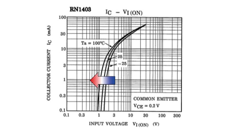
1. Input voltage (ON), VI(ON)
VI(ON) is the input voltage required for a transistor to pass the specified current under the specified conditions. To turn on the BRT without fail, it is necessary to apply a voltage higher than the maximum input voltage (ON) (VI(ON)) across the base (B) and emitter (E) terminals.
The IC – VI(ON) curves indicate that VI(ON) decreases as temperature increases.
| Characteristic | Symbol | Test Circuit |
Test Condition | Min | Typ. | Max | Unit | ||
|---|---|---|---|---|---|---|---|---|---|
| Input voltage (ON) | RN1401 | VI (ON) | — | VCE = 0.2 V, IC = 5 mA | 1.1 | — | 2.0 | V | |
| RN1402 | 1.2 | — | 2.4 | ||||||
| RN1403 | 1.3 | — | 3.0 | ||||||
| RN1404 | 1.5 | — | 5.0 | ||||||
| RN1405 | 0.6 | — | 1.1 | ||||||
| RN1406 | 0.7 | — | 1.3 | ||||||
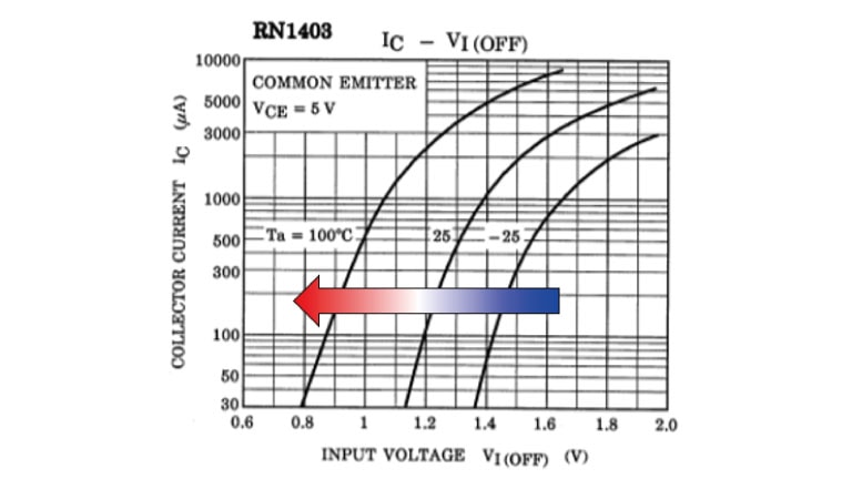
2. Input voltage (OFF), VI(OFF)
VI(OFF) is the input voltage required to meet the conditions under which a BRT is defined as off. To turn off the BRT without fail, it is necessary to apply a voltage lower than the minimum input voltage (OFF) (VI(OFF)) across the base (B) and emitter (E) terminals. As is the case with VI(ON), VI(OFF) decreases as temperature increases.
| Characteristic | Symbol | Test Circuit | Test Condition | Min | Typ. | Max | Unit | ||
|---|---|---|---|---|---|---|---|---|---|
| Input voltage (OFF) | RN1401 to 1404 | VI (OFF) | — | VCE = 5 V, IC = 0.1 mA | 1.0 | — | 1.5 | V | |
| RN1405, 1406 | 0.5 | — | 0.8 | ||||||
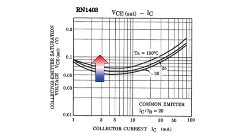
3. Collector-emitter saturation voltage, VCE(sat)
VCE(sat) is the collector-emitter voltage of the BRT when it is operating in the saturation region at the specified current. The VCE(sat) – IC curves indicate that VCE(sat) increases as temperature increases.
| Characteristic | Symbol | Test Circuit | Test Condition | Min | Typ. | Max | Unit | ||
|---|---|---|---|---|---|---|---|---|---|
Collector-emitter saturation voltage |
RN1401 to 1406 | VCE(SAT) | — | IC = 5 mA, IB = 0.25 mA | — | 0.1 | 0.3 | V | |
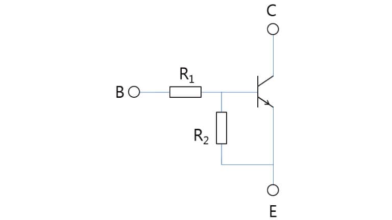
4. Input resistor, R1
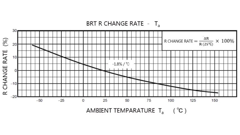
R1 is the value of a resistor in series with the base terminal of the BRT. In the case of the BRTs shown below, there is ±30% variation in R1. R1 affects VI(ON) and other characteristics. R1 decreases at a rate of roughly 0.2%/°C.
| Characteristic | Symbol | Test Circuit |
Test Condition | Min | Typ. | Max | Unit | ||
|---|---|---|---|---|---|---|---|---|---|
| Input resistor | RN1401 | R1 | — | — | 3.29 | 4.7 | 6.11 | kΩ | |
| RN1402 | 7 | 10 | 13 | ||||||
| RN1403 | 15.4 | 22 | 28.6 | ||||||
| RN1404 | 32.9 | 47 | 61.1 | ||||||
| RN1405 | 1.54 | 2.2 | 2.86 | ||||||
| RN1406 | 3.29 | 4.7 | 6.11 | ||||||
5. Resistor ratio, R1/R2
The resistor ratio (R1/R2) is the ratio of the R1 resistance to the R2 resistance. In the case of the BRTs shown below, there is ±10% variation in R1/R2. The value of the base-emitter resistor (R2) is not specified separately. Instead, the resistor ratio (R1/R2) is specified since it is more important.
| Characteristic | Symbol | Test Circuit |
Test Condition | Min | Typ. | Max | Unit | ||
|---|---|---|---|---|---|---|---|---|---|
| Resistor ratio | RN1401 to 1404 | R1/R2 | — | — | 0.9 | 1.0 | 1.1 | — | |
| RN1405 | 0.0421 | 0.0468 | 0.0515 | ||||||
| RN1406 | 0.09 | 0.1 | 0.11 | ||||||