


What is a MOSFET?
MOSFET (Metal-Oxide-Semiconductor Field-Effect Transistor) is a type of field-effect transistor that utilizes a metal oxide semiconductor and is an essential device for power electronics and high-speed switching applications.
Its basic structure consists of four terminals: Gate (G), Drain (D), Source (S), and Body (B), with the body typically connected to the source. The conduction state between the drain and source is controlled by the gate-to-source voltage (VGS). As a voltage-driven device, MOSFETs exhibit very low gate current, enabling low-loss operation. MOSFETs are classified by carrier type into N-channel (electrons) and P-channel (holes), and by operating mode into normally-off enhancement type and normally-on depletion type. Unlike bipolar transistors, which use both electrons and holes as carriers, MOSFETs use only one type, making them unipolar devices with superior high-speed switching performance.
Types of MOSFETs
MOSFETs are a type of transistor and are included in the field effect transistor (FET) category, as shown in Figure 1. MOSFETs are divided into enhancement and depletion types based on how they operate.
- Enhancement type: When the gate-source voltage VGS is 0V, the MOSFET is in the off state. It is also called a normally-off device because it is off when no bias is applied.
- Depletion type: When VGS is 0V, the MOSFET is in the on state. It is also called a normally-on device because it is on when no bias is applied.
In systems such as electronic devices, the control signal (gate voltage) may become "L" when a failure occurs. In switching and power switches (load switches), which are the main applications for MOSFETs, if the MOSFET becomes on (conducting) when a failure occurs, it can cause a safety problem. For this reason, the enhancement type is mainly used. In fact, most MOSFETs on the market are enhancement types.
Furthermore, these enhancement and depletion types are divided into P-type and N-type, respectively.
- P-type: When a MOSFET is turned on, the N-layer directly beneath the gate is inverted, creating a channel (inversion layer) with the same properties as a P-type semiconductor. The voltage condition for turning on is VG < VS, |VGS| > Vth. The majority carriers are holes.
- N-type: When a MOSFET is turned on, the P-layer directly beneath the gate is inverted, creating a channel (inversion layer) with the same properties as an N-type semiconductor. The voltage condition for turning on is VG >VS, |VGS| > Vth. The majority carriers are electrons.
From the perspective of physical properties, electrons have higher mobility than holes. Mobility is a measure that indicates how fast carriers (electrons and holes) can move in an electric field. In other words, high mobility increases the drift current. The effects on MOSFETs include ① a decrease in on-resistance (channel resistance), ② high-speed switching, and ③ an increase in drain current. Therefore, if the process is equivalent and the chip area built into the product is the same, N-type (N-ch) MOSFETs will have better characteristics.
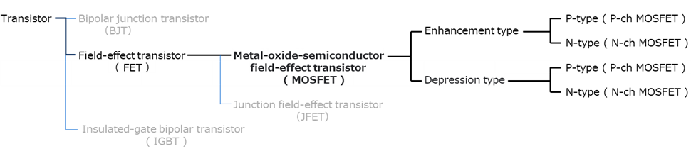
Figure 1 Classification of MOSFETs
Hierarchical classification of MOSFET starting from transistor at the top, branching into field-effect transistors (FET), MOSFET, operating modes (enhancement and depletion types), and channel polarity (P-type and N-type).
In addition, there are classifications such as horizontal and vertical depending on the manufacturing process. Please refer to the following FAQ. This document also explains the trench gate structure and super-junction structure.
FAQ: What types of structures are there in MOSFETs?
Basic structure and operation of MOSFET
The simplified structure and symbol of an enhancement-type N-ch MOSFET are shown in Figure 2, and the simplified structure and symbol of a depletion-type N-ch MOSFET are shown in Figure 3. In the depletion-type, there is a thin n-layer directly under the gate.
In an enhancement-type N-ch MOSFET, there are two n-type regions sandwiching a p-type region, and an electrode is placed across the n-type region, covered with an insulating film, and insulated from the others. Each region has an electrode, and the two terminals of the n-type region are called the source (S) and drain (D), and the electrode placed on the insulating film, which is the control terminal, is called the gate (G). The terminal on the back side is called the body (B) or backgate, and it is the terminal that determines the potential of the p-layer directly under the gate. In a normal discrete MOSFET (a standalone MOSFET element, not an IC), this terminal is connected to the source inside the package.
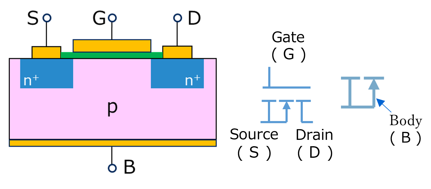
Figure 2 Enhancement type N-ch MOSFET
Illustration of the simplified structure and circuit symbol of an N-channel enhancement-mode MOSFET. It shows two n-type regions (source and drain) on a p-type substrate called the body, which typically connects to the source. The gate is placed over an insulating layer opposite the body. When voltage is applied to the gate, a channel forms, controlling current between drain and source.
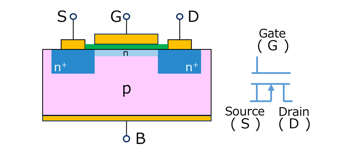
Figure 3 Depletion-type N-ch MOSFET
Illustration of the simplified structure and circuit symbol of an N-channel depletion-mode MOSFET. It shows two n-type regions (source and drain) on a p-type substrate, with a thin n-layer under the gate. Gate voltage modulates channel conductivity, controlling current between drain and source.
MOSFETs have three operating regions, as shown below. These regions refer to the ranges shown on the ID-VDS curve (Drain current vs Drain-Source voltage curve) in Figure 4, which is known as the static characteristics of MOSFETs.
- Cutoff region: Even if the drain-source voltage VDS is increased, the drain current ID does not flow.
- Linear region: ID flows in proportion to VDS.
- Saturation region: ID is not proportional to VDS. An almost constant ID flows, which depends on the gate-source voltage.
In the circuit shown in Figure 5, when VDS is applied between the drain and source and the gate-source voltage is gradually increased, the MOSFET turns on. The voltage at which the MOSFET turns on is called the gate threshold voltage Vth. Depending on the applied VDS voltage, it can be divided into a linear region and a saturation region.
- VDS < VGS - Vth: Turns on in the linear region
- VDS > VGS - Vth: Turns on in the saturation region
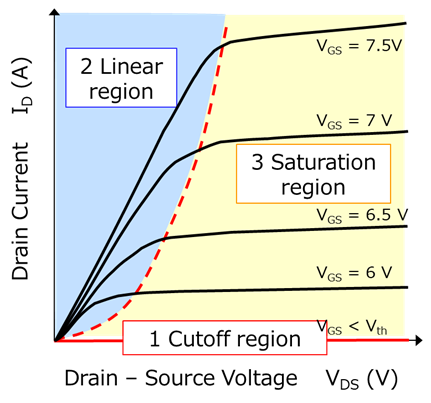
Figure 4 MOSFET static characteristics (ID - VDS curve)
Static characteristics of a MOSFET shown as an ID-VDS curve. The diagram illustrates the relationship between drain current (ID) and drain-to-source voltage (VDS), overlaid with three operating regions: cutoff, linear, and saturation.

Figure 5 MOSFET static characteristics measurement circuit
Basic MOSFET measurement circuit showing separate voltage sources applied between source-gate and source-drain to measure ID-VDS characteristics.
The physical properties of operation are explained in the following FAQ. Please refer to it.
Note on Threshold Voltage (Vth)
In this FAQ, Vth refers to the MOSFET gate threshold voltage—the gate-to-source voltage at which an inversion layer forms and the MOSFET turns on. This is different from the thermal voltage (approximately 26mV) commonly mentioned in BJT theory.
Applications of MOSFETs
MOSFETs are mainly used for power electronics-related switching applications, replacing bipolar transistors, due to their fast-switching speed and almost no gate current.
The fast-switching speed of MOSFETs allows for high frequencies to be used to miniaturize switching power supplies. They also do not have tail currents, which are an issue with bipolar devices such as bipolar transistors and IGBTs. MOSFETs also do not require gate current to maintain the on state. For these reasons, they are mainly used in applications that require compact size and low loss.
Figure 6 shows examples of applications.
The Reference Design Center below lists many applications using MOSFETs, such as power supplies, power management, and motor control. Please refer to these as well.
Reference Design Center
For switching power supplies, we have prepared basic power supply circuits that can be simulated in the user's design environment. By downloading them, you can shorten the time required for simulation and save time in pre-verification when selecting power MOSFETs. Please refer to this as well.
Switched Mode Power Supply Library
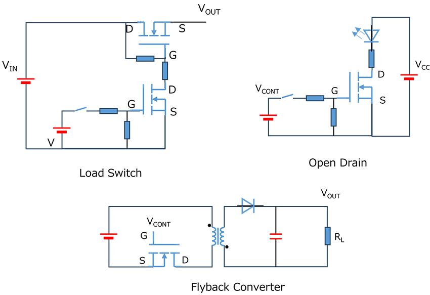
Figure 6 Example of a MOSFET circuit
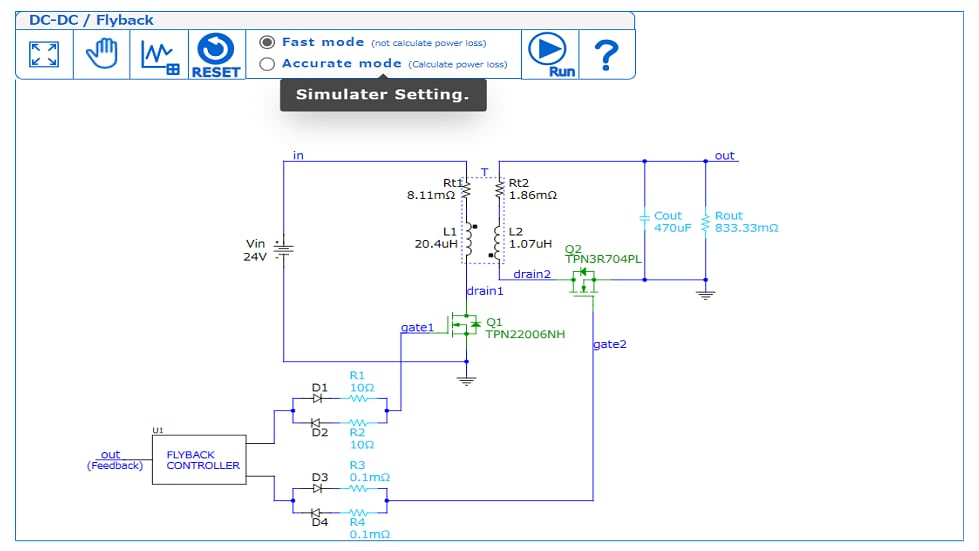
Representative MOSFET applications include a load switch used for power on/off control, an open-drain configuration used for digital signal level shifting and bus sharing, and a flyback converter used for isolated power conversion.
MOSFET packages
Toshiba's MOSFETs come in a wide variety of packages, from small packages for general-purpose applications to packages for power applications. We also offer composite products such as 2-in-1, which contains two MOSFETs. It is possible to select according to the purpose, heat dissipation, size, mounting method, etc.
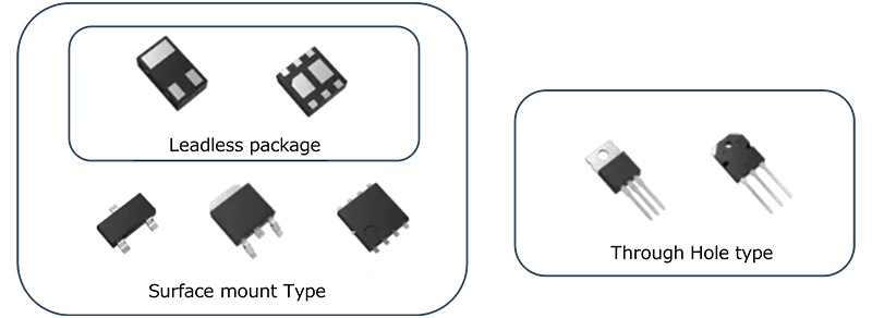
Figure 7 Example of a MOSFET package
Representative MOSFET package examples include surface-mount types and lead types, with leadless packages as part of the surface-mount group.
For details on the packages (dimensions and reference pad), please refer to the following page.
MOSFET package
Information such as a comparative simulation of temperature rise due to packages is available in the following application note. Please refer to it.
Hints and Tips for Thermal Design for Discrete Semiconductor Devices_part3
Related Links
Please refer to the following pages and documents for product lineup and other documents.
Parametric Search
MOSFETs
FAQs
Others
Online Circuit Simulator
The Online Circuit Simulator allows users to verify and select MOSFETs. (Members only)
* Company names, product names, and service names used in this FAQ may be of their respective companies.