
- General Top
- SEMICONDUCTOR
- STORAGE
- COMPANY
-
My ToshibaSemicon
- Semiconductor Top
-
ApplicationsAutomotive
Body Electronics
xEV
In-Vehicle Infotainment
Advanced Driver-Assistance Systems (ADAS)
Chassis
IndustrialInfrastructure
BEMS/HEMS
Factory Automation
Commercial Equipment
Consumer/PersonalIoT Equipment
Healthcare
Wearable Device
Mobile
Computer Peripherals
-
ProductsAutomotive Devices
Discrete Semiconductor
Diodes
Transistors
Logic ICs
Analog Devices
Digital Devices
Wireless Devices
※
 : Products list (parametric search)Power Semiconductors
SiC Power Devices
※
: Products list (parametric search)Isolators/Solid State RelaysPhotocouplers
Digital Isolators
Solid State Relays
Fiber Optic Transmitting Modules
※
: Products list (parametric search)MOSFETsIGBTs/IEGTsBipolar Transistors※
: Products list (parametric search)Diodes※
: Products list (parametric search)MicrocontrollersMotor Driver ICsIntelligent Power ICs※
: Products list (parametric search)Power Management ICsLinear ICs※
: Products list (parametric search)General Purpose Logic ICsLinear Image SensorsOther Product ICsOther Product ICs
※
: Products list (parametric search) -
Design & Development
-
Knowledge
- Where To Buy


- Part Number & Keyword Search
- Cross Reference Search
- Parametric Search
- Stock Check & Purchase
This webpage doesn't work with Internet Explorer. Please use the latest version of Google Chrome, Microsoft Edge, Mozilla Firefox or Safari.
require 3 characters or more. Search for multiple part numbers fromhere.
The information presented in this cross reference is based on TOSHIBA's selection criteria and should be treated as a suggestion only. Please carefully review the latest versions of all relevant information on the TOSHIBA products, including without limitation data sheets and validate all operating parameters of the TOSHIBA products to ensure that the suggested TOSHIBA products are truly compatible with your design and application.Please note that this cross reference is based on TOSHIBA's estimate of compatibility with other manufacturers' products, based on other manufacturers' published data, at the time the data was collected.TOSHIBA is not responsible for any incorrect or incomplete information. Information is subject to change at any time without notice.
require 3 characters or more.
What is the difference between MOSFETs and IGBTs?
MOSFETs and IGBTs are voltage-driven power semiconductor devices designed for different application ranges. In general, MOSFETs are used in low- to medium-voltage applications requiring high-speed switching, while IGBTs are widely used in high-voltage and high-current applications. These differences originate from their device structures and the way charge carriers behave during conduction. This FAQ compares the structure, operating principles, conduction characteristics, and switching characteristics of MOSFETs and IGBTs, and explains how to choose the appropriate device for a given application.
Structural Differences Between MOSFETs and IGBTs
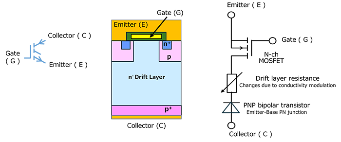
Both MOSFETs (Metal Oxide Semiconductor Field Effect Transistors) and IGBTs (Insulated Gate Bipolar Transistors) are voltage-driven power devices in which the current is controlled by an electrically insulated gate electrode. Both devices adopt a vertical structure in which current flows from the top surface to the backside of the chip, and the drift region (n⁻ layer) determines the voltage blocking capability.
The major structural difference between the two devices lies in the backside layer configuration of the drift region.
Figures 1 and 2 show the circuit symbols, device structures, and simplified equivalent circuits of MOSFETs and IGBTs.
In the simplified equivalent circuit of the MOSFET shown in Figure 1, the drift region resistance—which dominates the conduction characteristics of high-voltage MOSFETs—is represented in a simplified form.
In contrast, the simplified equivalent circuit of the IGBT in Figure 2 represents the minority carrier injection mechanism using a diode that corresponds to the pn junction between the p+ collector and the drift region, rather than depicting a full PNP transistor structure.
For more details on MOSFET structures, please refer to the following FAQ:
> What types of structures are there in MOSFETs?

Differences in Operating Principles Between MOSFETs and IGBTs
Due to their structural differences, MOSFETs and IGBTs differ in both the type of charge carriers involved in conduction and their carrier transport behavior.
Operating Principle of MOSFETs
In a MOSFET, applying a gate voltage forms a conductive channel between the source and drain, allowing current to flow.
During conduction, the current is carried only by majority carriers (electrons or holes).
Because MOSFETs operate exclusively with majority carriers, they are classified as unipolar devices, and no carrier storage occurs in the drift region.
As a result, MOSFETs can switch on and off rapidly, enabling high-speed switching operation.
For a detailed explanation of MOSFET operation, refer to the following FAQ:
> Understanding MOSFET Operation Principles and Mechanisms
Operating Principle of IGBTs
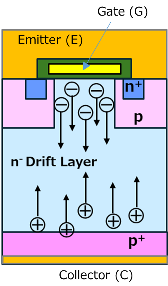
In addition to MOS gate channel control, IGBTs utilize minority carrier injection from a p⁺ layer located on the collector side into the drift region.
When a gate voltage is applied, a MOS channel is formed, and minority carriers (holes) are injected into the drift region from the p⁺ collector layer. At the same time, the formation of the MOS channel enables electrons to be supplied from the n⁺ emitter side.
As holes are injected into the drift region, it becomes necessary to maintain quasi-neutrality*, meaning that charge imbalance must be avoided within the semiconductor.
Consequently, the electron density in the drift region increases correspondingly, resulting in a state where both electrons and holes coexist at high densities.
Because both carrier types are present at high concentration, the conductivity of the drift region increases significantly.
This phenomenon is known as conductivity modulation.
Figure 3 schematically illustrates carrier behavior in the drift region during conductivity modulation, based on the structure shown in Figure 2. It shows injected holes from the collector side and electrons supplied from the emitter side coexisting simultaneously within the drift region.
Under normal conditions, carrier concentration in the drift region is determined by the doping concentration and remains in equilibrium. In IGBTs, however, minority carrier injection causes the carrier concentration to greatly exceed this equilibrium level.
This condition, in which injected carriers remain in the drift region for a certain period of time, is referred to as carrier storage.
For further details, see the following FAQ:
> What is conductivity modulation?
* : Quasi-neutrality refers to a condition within a semiconductor region in which the charges of electrons (−) and holes (+) almost cancel each other, resulting in negligible space charge.
Impact of Operating Principle Differences on Switching Characteristics
Because no carrier storage occurs in MOSFETs, turn-on and turn-off transitions follow changes in gate voltage almost immediately, enabling high-frequency switching.
In contrast, carrier storage occurs in the drift region of IGBTs. During turn-off, the stored minority carriers must be recombined or removed before the current can fully cease. As a result, current continues to flow for a short period after gate turn-off, and the switching speed becomes slower than that of MOSFETs.
This residual current component after turn-off is called tail current.
Tail current is a characteristic phenomenon observed during turn-off of IGBTs, which involve minority carrier storage due to bipolar operation, and it does not occur in unipolar devices such as MOSFETs.
Differences in Conduction Characteristics Between MOSFETs and IGBTs
In high-voltage MOSFETs, the drift region must be thick and lightly doped to achieve sufficient blocking capability. As a result, the resistance component of the drift region becomes the dominant part of the on-resistance, and the conduction voltage drop increases as the current increases.
In contrast, in IGBTs, minority carrier injection causes conductivity modulation, which significantly increases carrier density in the drift region.
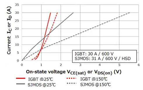
Figure 4 presents an example comparing the on-voltage characteristics of IGBTs and MOSFETs.
It shows that MOSFETs have lower on-voltage in the low-current region, whereas IGBTs exhibit lower VCE(sat) in the high-current region.
Thus, the distinct current-dependent behavior of the on-state voltage reflects a fundamental difference in the conduction characteristics of MOSFETs and IGBTs.
Figure 4 Notes
Figure 4 compares the on‑voltage characteristics of an IGBT and a high‑voltage MOSFET
(a Super‑junction MOSFET is shown here as a representative example).
The horizontal axis represents the on-state voltage—VDS(on) for the MOSFET and VCE(sat) for the IGBT—while the vertical axis represents conduction current. Characteristics at ambient temperatures of 25°C and 150°C are shown.
In the low-current region, the MOSFET on-voltage rises from nearly 0V. In contrast, the IGBT on-voltage starts at a higher value due to the voltage component originating from the pn junction, resulting in a forward-voltage offset similar to that of a diode.
In the high-current region, the slope of the IGBT characteristic becomes steeper, and above a certain current level, the IGBT exhibits a lower VCE(sat) than the MOSFET’s VDS(on).
For a detailed explanation of Super-junction MOSFET structures, please refer to the following FAQ:
> What types of structures are there in MOSFETs?
Summary: How to Choose Between MOSFETs and IGBTs
Due to differences in structure and operating principles, MOSFETs and IGBTs exhibit different trade-offs in conduction and switching characteristics.
MOSFETs are well suited for low- to medium-voltage applications that require low on-resistance and high-speed switching, particularly in high-frequency operation.
IGBTs, on the other hand, provide superior conduction performance under high-voltage and high-current conditions due to minority carrier injection and conductivity modulation.
However, attention must be paid to switching speed due to tail current caused by carrier storage.
By considering voltage level, current magnitude, and switching frequency requirements, the appropriate device can be selected based on a clear understanding of these trade-offs.
Typical application domains include:
- MOSFETs
Low- to medium-voltage applications requiring high-speed switching
(e.g., switching power supplies, DC-DC converters, high-frequency circuits) - IGBTs
High-voltage and high-current applications with relatively low switching frequency
(e.g., inverters, motor drives, industrial power conversion systems)
Understanding the trade-offs among conduction characteristics (RDS(on) / VCE(sat)), conduction loss, and switching loss is essential for selecting the most suitable device for each application.
| BJT | MOSFET | IGBT | |
|---|---|---|---|
| Drive type | Current drive |
Voltage drive |
Voltage drive |
| Power for driving | High | Low | Low |
| On state voltage | Moderate | Tends to increase in |
Low |
| Switching speed | Low |
High |
Moderate |
| Temperature stability | Poor | Good | Good |
| Difficulty of achieving high breakdown voltage |
Moderate | High | Easy with conductivity modulation |
Related Links
The following documents also contain related information.
Parametric Search
IGBTs/IEGTs
FAQs
* Company names, product names, and service names used in this FAQ may be of their respective companies.