
- General Top
- SEMICONDUCTOR
- STORAGE
- COMPANY
-
My ToshibaSemicon
- Semiconductor Top
-
ApplicationsAutomotive
Body Electronics
xEV
In-Vehicle Infotainment
Advanced Driver-Assistance Systems (ADAS)
Chassis
IndustrialInfrastructure
BEMS/HEMS
Factory Automation
Commercial Equipment
Consumer/PersonalIoT Equipment
Healthcare
Wearable Device
Mobile
Computer Peripherals
-
ProductsAutomotive Devices
Discrete Semiconductor
Diodes
Transistors
Logic ICs
Analog Devices
Digital Devices
Wireless Devices
※
 : Products list (parametric search)Power Semiconductors
SiC Power Devices
※
: Products list (parametric search)Isolators/Solid State RelaysPhotocouplers
Digital Isolators
Solid State Relays
Fiber Optic Transmitting Modules
※
: Products list (parametric search)MOSFETsIGBTs/IEGTsBipolar Transistors※
: Products list (parametric search)Diodes※
: Products list (parametric search)MicrocontrollersMotor Driver ICsIntelligent Power ICs※
: Products list (parametric search)Power Management ICsLinear ICs※
: Products list (parametric search)General Purpose Logic ICsLinear Image SensorsOther Product ICsOther Product ICs
※
: Products list (parametric search) -
Design & Development
-
Knowledge
- Where To Buy


- Part Number & Keyword Search
- Cross Reference Search
- Parametric Search
- Stock Check & Purchase
This webpage doesn't work with Internet Explorer. Please use the latest version of Google Chrome, Microsoft Edge, Mozilla Firefox or Safari.
require 3 characters or more. Search for multiple part numbers fromhere.
The information presented in this cross reference is based on TOSHIBA's selection criteria and should be treated as a suggestion only. Please carefully review the latest versions of all relevant information on the TOSHIBA products, including without limitation data sheets and validate all operating parameters of the TOSHIBA products to ensure that the suggested TOSHIBA products are truly compatible with your design and application.Please note that this cross reference is based on TOSHIBA's estimate of compatibility with other manufacturers' products, based on other manufacturers' published data, at the time the data was collected.TOSHIBA is not responsible for any incorrect or incomplete information. Information is subject to change at any time without notice.
require 3 characters or more.
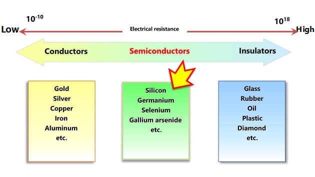
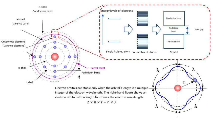
1-3. pn junction
Before discussing Schottky barrier diodes (SBDs), let us learn how a pn junction works since it is the most basic junction for forming a diode.
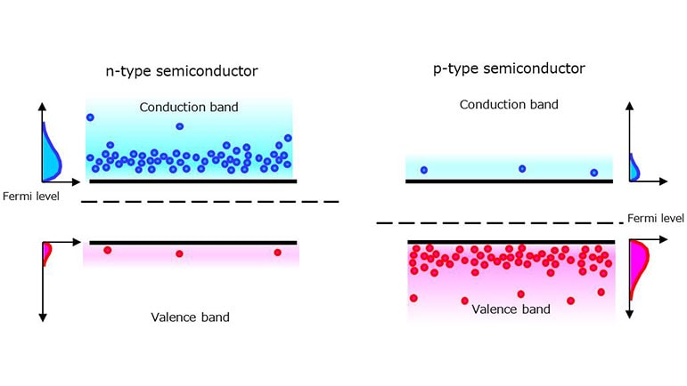
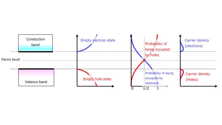
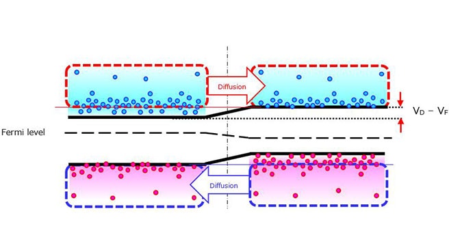
When p-type and n-type semiconductors are joined together, their Fermi levels become equal. This creates a difference in potential between the lower edges of the conduction bands of the n-type and p-type semiconductors (VCN and VCP respectively). This difference in potential is called the diffusion potential (VD) or built-in potential.
Electrons are the majority charge carriers in the n-type semiconductor whereas holes are the majority charge carriers in the p-type semiconductor. Near the junction, electrons in the n-type semiconductor and holes in the p-type semiconductor are attracted and bound to each other and disappear, creating a region called a depletion layer where no carrier exists. Then, some electrons in the n-type semiconductor diffuse into the p-type semiconductor as they have energy exceeding VD. Therefore, above VD, the electron densities in both semiconductors become equal. Likewise, some holes in the p-type semiconductor diffuse into the n-type semiconductor. The current that flows as a result of diffusion of charge carriers (electrons and holes) is called diffusion current. The application of voltage (i.e., an electric field) across the junction also causes drift current to flow. However, the diffusion current is dominant except in a depletion region. When the pn junction is unbiased, current stops flowing once the junction reaches an equilibrium state.


Chapter1 Basics of Schottky Barrier Diodes (Basic of Semiconductor Device)

Related information
- Products
Schottky Barrier Diodes - Applidcation Notes
Application Notes - FAQs
Diodes - Parametric Search
Schottky Barrier Diodes - Stock Check & Purchase
Stock Check & Purchase