
- General Top
- SEMICONDUCTOR
- STORAGE
- COMPANY
-
My ToshibaSemicon
- Semiconductor Top
-
ApplicationsAutomotive
Body Electronics
xEV
In-Vehicle Infotainment
Advanced Driver-Assistance Systems (ADAS)
Chassis
IndustrialInfrastructure
BEMS/HEMS
Factory Automation
Commercial Equipment
Consumer/PersonalIoT Equipment
Healthcare
Wearable Device
Mobile
Computer Peripherals
-
ProductsAutomotive Devices
Discrete Semiconductor
Diodes
Transistors
Logic ICs
Analog Devices
Digital Devices
Wireless Devices
※
 : Products list (parametric search)Power Semiconductors
SiC Power Devices
※
: Products list (parametric search)Isolators/Solid State RelaysPhotocouplers
Digital Isolators
Solid State Relays
Fiber Optic Transmitting Modules
※
: Products list (parametric search)MOSFETsIGBTs/IEGTsBipolar Transistors※
: Products list (parametric search)Diodes※
: Products list (parametric search)MicrocontrollersMotor Driver ICsIntelligent Power ICs※
: Products list (parametric search)Power Management ICsLinear ICs※
: Products list (parametric search)General Purpose Logic ICsLinear Image SensorsOther Product ICsOther Product ICs
※
: Products list (parametric search) -
Design & Development
-
Knowledge
- Where To Buy


- Part Number & Keyword Search
- Cross Reference Search
- Parametric Search
- Stock Check & Purchase
This webpage doesn't work with Internet Explorer. Please use the latest version of Google Chrome, Microsoft Edge, Mozilla Firefox or Safari.
require 3 characters or more. Search for multiple part numbers fromhere.
The information presented in this cross reference is based on TOSHIBA's selection criteria and should be treated as a suggestion only. Please carefully review the latest versions of all relevant information on the TOSHIBA products, including without limitation data sheets and validate all operating parameters of the TOSHIBA products to ensure that the suggested TOSHIBA products are truly compatible with your design and application.Please note that this cross reference is based on TOSHIBA's estimate of compatibility with other manufacturers' products, based on other manufacturers' published data, at the time the data was collected.TOSHIBA is not responsible for any incorrect or incomplete information. Information is subject to change at any time without notice.
require 3 characters or more.
Are there board design considerations for adding ESD protection diodes?
Electrostatic discharge (ESD) is a very short duration pulse. Performance cannot be fully demonstrated unless the board is designed with high frequency in mind. Here, we will explain the points to be noted in board design.
ESD protection diodes are widely used for protection against electrostatic discharge (ESD). Upon ESD entry, ESD protection diodes turn on immediately with low resistance to protect a device under protection (DUP).
As is the case with other types of protection devices, ESD protection diodes require several considerations for board design, including their placement and board trace layout. The following summarizes board design considerations, each of which is explained in greater detail later.
- Place ESD protection diodes as close as possible to a connector (to minimize the length of the L1 and L3 traces).
- Reduce the length of L2 following an ESD protection diode. Do not add any via holes along L2because they have large inductance.
- Reduce the ground impedance of L5 between a DUP (“IC” in Figure 3) and the ESD entry point(e.g., a connector).
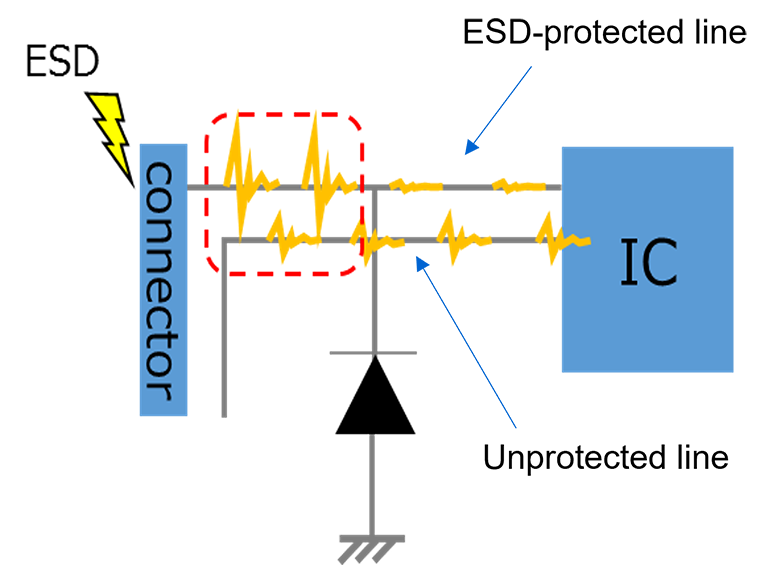
- Do not run ESD-protected lines connected to an ESD entry point (e.g., a connector) in parallel with any lines that are not protected from ESD. These lines should not run in parallel particularly from the ESD entry point to the ESD protection diode. (See Figure 6.)
As is the case with Zener diodes, ESD protection diodes capitalize on the reverse characteristics of a pn junction. As the reverse voltage across the pn junction diode is increased, avalanche breakdown occurs at some point called Zener voltage (VZ). Because of this characteristic, ESD protection diodes remain off during normal operation of a system and turn on immediately upon ESD entry, reducing the ESD energy applied to the DUP.
To realize low capacitance and dynamic resistance, Toshiba’s ESD protection diodes are optimized for ESD protection based on its Zener diode technology cultivated for decades.
Figure 1 shows an example of a circuit with an ESD protection diode.
Main ESD entry points are externally exposed ports for USB, HDMI, and other cables. Therefore, ESD protection diodes are connected between ground and the signal or control lines from these I/O ports. Let the ESD voltage upon entry be VESD. Then, VESD is applied across the ESD protection diode and the DUP.
The ESD current applied to the DUP (IProt) depends on the internal circuitry, but the higher the VESD, the higher the IProt. An ESD strike could degrade or destroy the DUP. The cause of the DUP degradation or destruction can be excessive voltage, current, or energy. In any case, reducing VESD is the key to improving ESD protection performance.
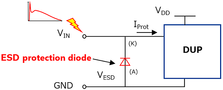
To reduce VESD, it is important to select an ESD protection diode with low clamp voltage (VC) and dynamic resistance (RDYN). For a description of clamp voltage and dynamic resistance, see the FAQ entries “How do ESD protection diodes operate?” and “How do I choose an ESD protection diode?.”
How do ESD protection diodes operate?
How do I choose an ESD protection diode?
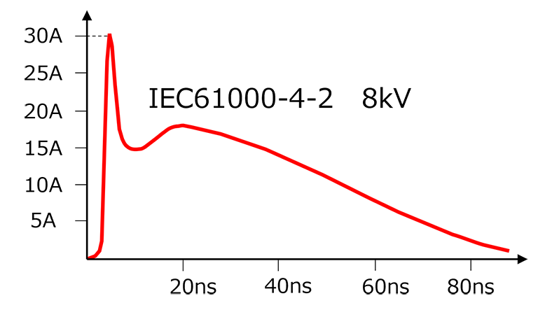
However, selecting the right ESD protection diode is only the first step. The above considerations are sufficient for direct current, but not for high-frequency pulses. As you know, ESD is a high-frequency pulse. For example, the following shows a test waveform specified in IEC 61000-4-2, an ESD immunity test standard.
Board design is important for high-frequency pulses. Since board traces and via holes (through-holes) act as inductance, it is necessary to minimize the lengths of traces from possible ESD entry points (e.g., connectors) to ESD protection diodes without running them through via holes. In addition, be sure to remember that ground traces should be as wide as possible to reduce their impedance. Now, let us use illustrations to discuss the considerations for board design.
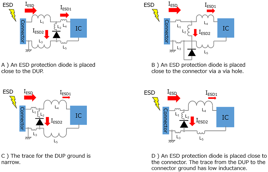
Figure 3 shows four placement options for an ESD protection diode.
A) An ESD protection diode is placed close to the DUP.
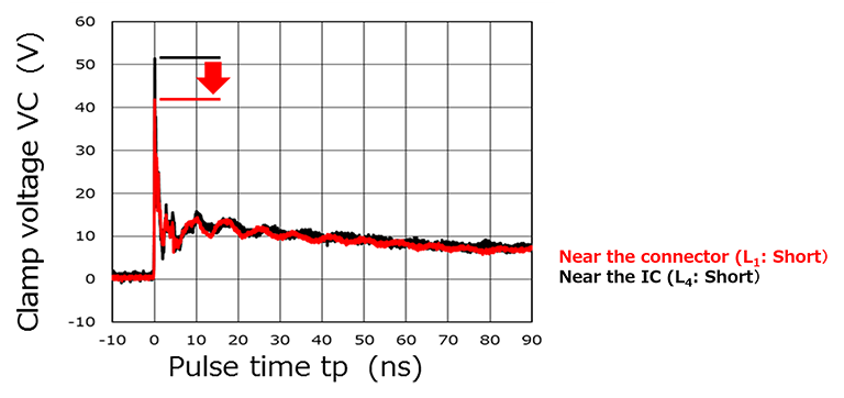
The board traces leading to the ESD protection diode and the DUP have almost the same impedance. A high-frequency ESD pulse that enters a board is affected by inductance before being applied to the ESD protection diode and the DUP. Therefore, the inductance makes the rising slope of the ESD pulse slightly shallower, causing the ESD protection diode to turn on more slowly. Look at Figure 4. When an ESD protection diode is placed close to the connector, the voltage across the DUP or the first peak voltage immediately after an ESD strike is lower than in the case in which it is placed close to the DUP.
B) An ESD protection diode is placed close to the connector using a via hole.
The ESD pulse is affected by the number and sizes of via holes. Using via holes is equivalent to increasing the length of the trace leading to the ESD protection diode. Therefore, wherever the use of via holes can be avoided, it is advisable not to use them.
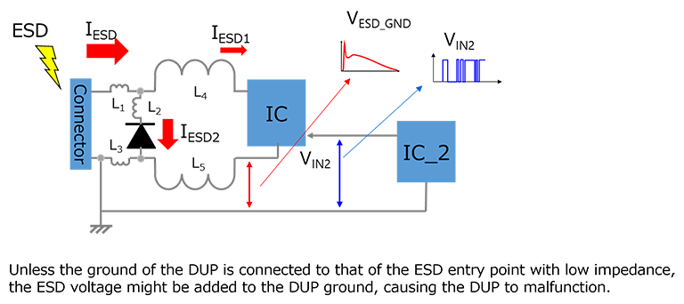
C) An ESD protection diode is placed close to the connector, but the trace from the DUP ground to the connector ground has high inductance.
L1 and L3 do not affect the rise of the ESD pulse. However, if L5 is large, the DUP might malfunction.Look at Figure 5. When an ESD pulse enters a board, the clamp voltage of the ESD protection diode is divided by L4, L5, and ZIC (i.e., the input impedance that the DUP has at the time of ESD entry). This causes the GND potential of the DUP to rise by the number of volts across L5. If VIN2 is applied from IC_2 that is free from any effects of ESD, the VIN2 potential with reference to the ground of the DUP becomes VIN2-VESD_GND and causes it to malfunction. To prevent this, the impedance of the ground trace from the ESD entry point to the DUP should be sufficiently low.
D) An ESD protection diode is placed close to the connector. The trace from the DUP to the connector ground has low inductance.
This is the ideal placement.
It is also risky to run an ESD-susceptible line in parallel with a signal line connected to a connector. ESD might cause the line voltage to rise because of capacitive coupling or electromagnetic induction, causing the DUP to be degraded or destroyed.
Related Links
For TVS diode (ESD protection diode) products, please refer to the following links.
* The terms HDMI, and HDMI High-Definition Multimedia Interface, and the HDMI Logo are trademarks or registered trademarks of HDMI Licensing Administrator, Inc. in the United States and other countries.
* Other company names, product names, and service names may be trademarks of their respective companies.