
- General Top
- SEMICONDUCTOR
- STORAGE
- COMPANY
-
My ToshibaSemicon
- Semiconductor Top
-
ApplicationsAutomotive
Body Electronics
xEV
In-Vehicle Infotainment
Advanced Driver-Assistance Systems (ADAS)
Chassis
IndustrialInfrastructure
BEMS/HEMS
Factory Automation
Commercial Equipment
Consumer/PersonalIoT Equipment
Healthcare
Wearable Device
Mobile
Computer Peripherals
-
ProductsAutomotive Devices
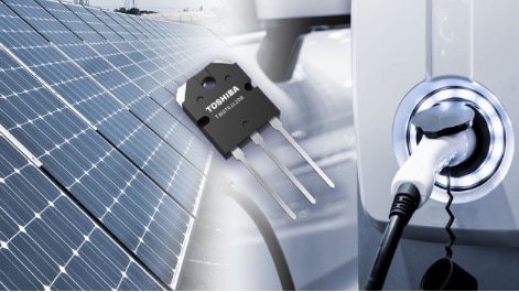
Discrete Semiconductor
Diodes
Transistors
Logic ICs
Analog Devices
Digital Devices
Wireless Devices
※
 : Products list (parametric search)Power Semiconductors
SiC Power Devices
※
: Products list (parametric search)Isolators/Solid State RelaysPhotocouplers
Digital Isolators
Solid State Relays
Fiber Optic Transmitting Modules
※
: Products list (parametric search)MOSFETsIGBTs/IEGTsBipolar Transistors※
: Products list (parametric search)Diodes※
: Products list (parametric search)MicrocontrollersMotor Driver ICsIntelligent Power ICs※
: Products list (parametric search)Power Management ICsLinear ICs※
: Products list (parametric search)General Purpose Logic ICsLinear Image SensorsOther Product ICsOther Product ICs
※
: Products list (parametric search) -
Design & Development
-
Knowledge
- Where To Buy


- Part Number & Keyword Search
- Cross Reference Search
- Parametric Search
- Stock Check & Purchase
This webpage doesn't work with Internet Explorer. Please use the latest version of Google Chrome, Microsoft Edge, Mozilla Firefox or Safari.
require 3 characters or more. Search for multiple part numbers fromhere.
The information presented in this cross reference is based on TOSHIBA's selection criteria and should be treated as a suggestion only. Please carefully review the latest versions of all relevant information on the TOSHIBA products, including without limitation data sheets and validate all operating parameters of the TOSHIBA products to ensure that the suggested TOSHIBA products are truly compatible with your design and application.Please note that this cross reference is based on TOSHIBA's estimate of compatibility with other manufacturers' products, based on other manufacturers' published data, at the time the data was collected.TOSHIBA is not responsible for any incorrect or incomplete information. Information is subject to change at any time without notice.
require 3 characters or more.
What is avalanche in MOSFET? (avalanche capability)
When a MOSFET is turned off, an avalanche breakdown occurs if the voltage applied between the drain and source exceeds the absolute maximum rating VDSS. Even if the DC voltage of the drain is within the rating, a surge voltage may be superimposed on this DC voltage due to factors such as stray inductance in the wiring, causing it to exceed the maximum rating. During an avalanche breakdown, a current flows suddenly, which may lead to avalanche destruction. When designing a circuit, you should select a MOSFET with a drain-source voltage VDSS that has a sufficient margin for the maximum drain voltage, even though there are products with guaranteed avalanche capability. Also, take the measures described below to prevent surge voltages from occurring.
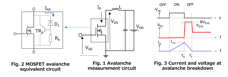
Avalanche breakdown of MOSFET
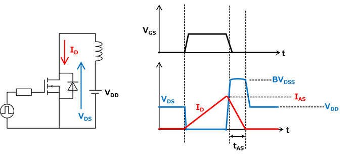
During the transitional timing when a MOSFET goes from on to off, a surge voltage may be applied between the drain and source due to the influence of parasitic inductance in the circuit. (See Fig. 1)
When this surge voltage is applied as a reverse bias to the MOSFET , free electrons in the pn junction of the internal parasitic diode (refer to Fig. 2 the equivalent circuit) are accelerated and gain high kinetic energy.
These high-energy electrons collide with atoms, releasing additional free electrons and generating electron-hole pairs. The newly generated electrons are also accelerated by the high electric field, creating more electron-hole pairs in a chain reaction. As a result, the current rapidly increases, and a large current—known as avalanche current (IAS)—flows. This phenomenon is called avalanche breakdown.
For more information on avalanche breakdown, please refer to section 2.4 "Zener Diodes" in the referenced document.
Application Note: Basics of Diodes (Types and Overview of Diodes) (1.8MB)

About Avalanche Breakdown
Avalanche breakdown can be classified into two main types: thermal breakdown and current-induced breakdown caused by a parasitic transistor.
1. Thermal Breakdown
Fig. 4 shows an avalanche test circuit and its waveform. In this circuit, when the MOSFET turns off, the inductance L attempts to maintain the current that was previously flowing. As a result, a reverse voltage is generated by the inductance, and if the drain-source voltage exceeds the rated VDSS, avalanche breakdown may occur.
During this breakdown period, avalanche current (IAS) flows through the MOSFET. The device experiences power loss due to the combination of this avalanche current and the breakdown voltage BVDSS. This power loss causes the junction temperature Tj of the device to rise, potentially leading to device failure. This energy loss is referred to as avalanche energy (EAS) and is an important parameter in circuit design.

The avalanche energy is given by:

EAS: Avalanche energy IAS: Avalanche current BVDSS: Drain-source breakdown voltage
VDD: Power supply voltage tAS: Avalanche period PA: Power during avalanche L: Inductance
2. Current Destruction Caused by a Parasitic Transistor
When the drain-source voltage of a MOSFET exceeds its rated VDSS and avalanche breakdown occurs, avalanche current (IAS) flows into the internal resistance RBE, as shown in Fig. 3. This causes a voltage to develop across the base-emitter junction of the parasitic bipolar transistor (BJT), expressed as:
VBE=IAS×RBE
f this VBE becomes sufficiently large, the parasitic transistor turns on, allowing a large current (short-circuit current) to flow. This can lead to catastrophic failure of the MOSFET due to short-circuit destruction.
Countermeasures Against Avalanche Breakdown
To prevent MOSFET damage caused by avalanche breakdown, the following countermeasures are effective:
・Selecting Devices with Sufficient Margin:
Choose MOSFETs with a drain-source voltage rating (VDSS) that includes a sufficient margin above the maximum voltage expected to be applied.
Some products guarantee avalanche tolerance as part of their absolute maximum ratings, including allowable single-pulse current and energy. An example is shown below:
| Item | Symbol | Rating | Unit |
|---|---|---|---|
| Single-pulse avalanche energy (Note) | EAS | 1049 |
mJ |
| Single-pulse avalanche current | IAS | 8.0 | A |
Note :VDD = 90V, Tch = 25℃ (initial), L = 29mH, IAS = 8.0A
・Minimizing Parasitic Inductance in Wiring:
Keep the wiring to the load (current-carrying paths) as short and thick as possible.
Using compact or surface-mount packages can also reduce lead inductance.
・Increasing Gate Resistor Value:
By increasing the gate resistance, the switching speed is reduced, which lowers the rate of change in drain current (di/dt).
The surge voltage VS is determined by the following formula:
VS = LS * di/dt
Reducing di/dt helps suppress surge voltage.
However, slower switching increases the transition time from on to off, which can lead to higher switching losses. Therefore, select an optimal gate resistance value that balances surge suppression and power loss.
・Using Snubber or Clamp Circuits:
These circuits help suppress surge voltages that occur when the MOSFET switches from on to off. They absorb the energy stored in parasitic inductance, protecting the device from overvoltage stress.
Related Links
The following documents also contain related information.
Parametric Search
MOSFETs
FAQs
* Company names, product names, and service names used in this FAQ may be of their respective companies.