
- General Top
- SEMICONDUCTOR
- STORAGE
- COMPANY
-
My ToshibaSemicon
- Semiconductor Top
-
ApplicationsAutomotive
Body Electronics
xEV
In-Vehicle Infotainment
Advanced Driver-Assistance Systems (ADAS)
Chassis
IndustrialInfrastructure
BEMS/HEMS
Factory Automation
Commercial Equipment
Consumer/PersonalIoT Equipment
Healthcare
Wearable Device
Mobile
Computer Peripherals
-
ProductsAutomotive Devices
Discrete Semiconductor
Diodes
Transistors
Logic ICs
Analog Devices
Digital Devices
Wireless Devices
※
 : Products list (parametric search)Power Semiconductors
SiC Power Devices
※
: Products list (parametric search)Isolators/Solid State RelaysPhotocouplers
Digital Isolators
Solid State Relays
Fiber Optic Transmitting Modules
※
: Products list (parametric search)MOSFETsIGBTs/IEGTsBipolar Transistors※
: Products list (parametric search)Diodes※
: Products list (parametric search)MicrocontrollersMotor Driver ICsIntelligent Power ICs※
: Products list (parametric search)Power Management ICsLinear ICs※
: Products list (parametric search)General Purpose Logic ICsLinear Image SensorsOther Product ICsOther Product ICs
※
: Products list (parametric search) -
Design & Development
-
Knowledge
- Where To Buy


- Part Number & Keyword Search
- Cross Reference Search
- Parametric Search
- Stock Check & Purchase
This webpage doesn't work with Internet Explorer. Please use the latest version of Google Chrome, Microsoft Edge, Mozilla Firefox or Safari.
require 3 characters or more. Search for multiple part numbers fromhere.
The information presented in this cross reference is based on TOSHIBA's selection criteria and should be treated as a suggestion only. Please carefully review the latest versions of all relevant information on the TOSHIBA products, including without limitation data sheets and validate all operating parameters of the TOSHIBA products to ensure that the suggested TOSHIBA products are truly compatible with your design and application.Please note that this cross reference is based on TOSHIBA's estimate of compatibility with other manufacturers' products, based on other manufacturers' published data, at the time the data was collected.TOSHIBA is not responsible for any incorrect or incomplete information. Information is subject to change at any time without notice.
require 3 characters or more.
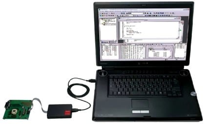
TX19A/H1 Series Development System
Light On-Chip Debug Emulation System
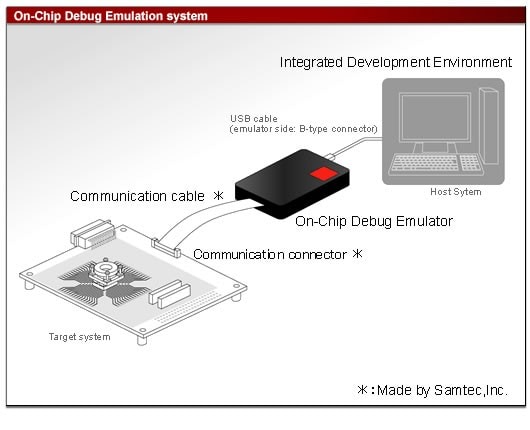
The RTE19A/H1 On-Chip Debug Emulation System consists of Integrated Development Environment, RTE19 Light On-Chip Debug Emulator and a communication cable. It provides various debug functions by controlling the on-chip debug function of the microcomputer mounted onto the target system.
- Capable of debugging in the operating condition equivalent to the MCU installed product.
- Real-time PC/PD trace.
- Trace control using an event feature.
- Capable of referring to the memory during program execution.
Check the product names and numbers at this website
The product information is also provided in "Comprehensive List (Microcomputers)" under "Document" for your use.
| Host interface | USB2.0 High-speed | |
|---|---|---|
| Emulation memory | internal FLASH ROM | |
| Event | Number of points | PC bus: 8 points Data bus: 4 points |
| Comparison items | Address, data, status | |
| Comparison conditionscondition | Match, unmatch (Notes-1) | |
| Pass count | Once | |
| Event trigger actions | Break, trace control, timer control, memory write, memory read | |
| Event combinations | OR | |
| Hardware break | PC bus: 8 points (Notes-2) | |
| Software break | 256 points(settable only on RAM) | |
| Trace memory Capacity | 256 frames (Notes-3) | |
| Trace memory Modes | Free trace, trigger trace | |
| Trace items | PC address, data address, data value, status, tag timer | |
| Trace overflow actions | Overwriting, overwriting prohibit, break | |
| Timer measurement | Lap timer: 1 channel | |
| Memory access | Memory display during program execution | Variables: 16 bytes x 32 Memory: Up to 1024 bytes |
| Memory rewrite during program execution | 4 bytes × 4 block can be written simultaneously. | |
| Program variables | Display | Binary, octal, decimal or hexadecimal display can be selected for each variable. |
| Registration | Variables, arrays, structures and unions can be registered by the elements. | |
| Sauce display | - Source - Source + assembler code - Source + assembler code + machine language |
|
| External output | - | |
| External input | - | |
| Performance analysis: Module time measurement | - | |
| Performance analysis: Coverage measurement | - | |
| Flash programming/security feature | Internal/external Flash memory can be programmed during debugging. | |
(Notes-1) Only data bus comparison is unmatch.
(Notes-2) Shared with event break.
(Notes-3) There are some cases where the trace memory capacity varies by a tracing condition or operating status.
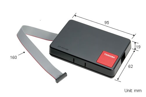
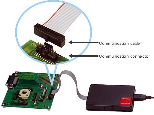
Product Configuration and Appearance of RTE19 Light On-Chip Debug Emulator
Content of Product
- RTE19 Light On-Chip Debug Emulator main body
- Communication cable (already connected to the emulator main body) (Notes)
- Communication connector (Notes)
- One license for downloading the Integrated Development Environment from website.
- (Notes) Made by Samtec,Inc.
Items to Be Prepared by Customer
- Host system
- USB cable (emulator side: B-type connector、USB2.0 compatible)
- Microcomputer on the target system (with on-chip debug function incorporated)
About Connection to Target System
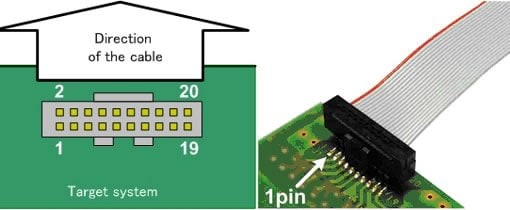
Seeing the following pin assignment table, etc., lay out/mount the Communication Connector (FTSH series 20pin connector made by Samtec, Inc.) on to the target system where the On-chip debug emulation system is to be connected.
One Communication Connector comes with an emulator, but those of the identical series (FTSH series) released from Samtec, Inc. are also available.
FTSH-110-01-[*]-[*][*]-[*][*]
[*] of the part number indicates a connector option. When purchasing, choose a suitable option according to its usage. For details specifications, please visit Samtec, Inc. website.
Communication Connector attached to an Emulator
| Part Nnumber | Note |
|---|---|
| FTSH-110-01-L-DV-K | Surface mount type with keying shroud |
Communication Connector Pin Assignment Table
| Connector Pin No. | Signal Name |
Remark |
|---|---|---|
| 1 | /TRST | (Note-1) |
| 3 | TDI | - |
| 5 | TDO | - |
| 7 | TMS | - |
| 9 | TCK | - |
| 11 | /RESET | (Note-1) (open drain) |
| 13 | /DINT | - |
| 15 | /EJE | - |
| 17 | - | Not use |
| 19 | - | Not use |
| Connector Pin No. | Signal Name | Remark |
|---|---|---|
| 2 | GND | - |
| 4 | GND | - |
| 6 | GND | - |
| 8 | GND | - |
| 10 | GND | - |
| 12 | - | Not use |
| 14 | VCC | (Note-1) |
| 16 | GND |
- |
| 18 | GND |
- |
| 20 | GND |
- |
(Note-1) Refer to the following points of concern in signal wiring.
Note for Layout of Communication Cable Connector
The following figure shows the cable pull-out direction and connector pin position, when the emulator is connected. To design the board, take into account interference with other parts at the time of connecting the communication cable. For a connector size, please visit Samtec, Inc. website.
Points of concern in signal connection
- When a /TRST (Test Reset for JTAG) terminal does not exist in MCU, /TRST of the EJTAG connector need not be connected.
- Connect /RESET of a connector directly to the /RESET pin of the MCU, connecting wired-OR with output of a reset circuit on a target board. The emulator drives a /RESET signal in order to control resetting of the target system. If the capacity of the reset circuit on the target board is too large or /RESET of the connector is not directly connected to the /RESET pin of the MCU, resetting of the target system may not be successfully controlled.
If reset control of the target system is not required, it is needless to connect /RESET of the connector to the /RESET pin of the MCU. In this case, the emulator can control resetting of a microcomputer alone. - Connect VCC of the connector to a power pin for the EJTAG pin of the MCU. VCC is used as a power input pin for driving/monitoring an EJTAG signal.
Points of concern in signal wiring
- Locate the connector within 10cm (4 inches) from the MCU. Specially, wiring the same length in TDI, TDO, TMS and TCK signals. If the connector is located further than 10cm (4 inches) away from the MCU or the length of each signals wire differ extremely, Emulator may not work correctly.
- Please make VCC/GND wiring between the MCU and the connector into the shortest distance. (Less than 5cm. Even if long, it is less than 10cm.) If VCC/GND wiring becomes long, it may not operate correctly.
About Emulation Operating Voltage/Frequency
- Any operating frequency and operating voltage in the device operation assurance range is available.
- Note that the power/clock cannot be supplied from the emulator to the target system.
Limitation of the On-Chip Debug Emulation
- When connecting an on-chip debug emulator to a debug target system, communication pins are not available as a combined feature because they are occupied by the emulator.
Precautions for USB Connection
- The emulator is connected to the host system via the USB. (USB2.0 High-speed)
- To newly connect the emulator to the host system, it is necessary to install a USB driver.
Accessory
Communication Cable
The communication cable is used to connect the emulator or the FLASH Writer to the target system. It is pre-plugged to the emulator or the FLASH Writer.
The communication cable is available from Samtec, Inc. For detailed specifications, please visit Samtec, Inc. website.
The recommended product can also be purchased from the following agencies.
| Name | Part Number | Remark |
|---|---|---|
| Communication cable |
FFSD-10-D-07.00-01-N | Pre-plugged to the emulator or the FLASH Writer |
Communication Connector
The communication connector is used to connect the emulator or the FLASH Writer to the target system. The part numbers shown below are examples. Other mount types, such as through-hole, and other mating options are also available to meet the specific needs of each customer.
The communication connector is available from Samtec, Inc. For detailed specifications, please visit Samtec, Inc. website.
The recommended product can also be purchased from the following agencies.
| Name | Part Number | Remark |
|---|---|---|
| Communication connector | FTSH-110-01-L-DV-K | Surface mount type with keying shroud. Each emulator comes with one communication connector. |