
- General Top
- SEMICONDUCTOR
- STORAGE
- COMPANY
-
My ToshibaSemicon
- Semiconductor Top
-
ApplicationsAutomotive
Body Electronics
xEV
In-Vehicle Infotainment
Advanced Driver-Assistance Systems (ADAS)
Chassis
IndustrialInfrastructure
BEMS/HEMS
Factory Automation
Commercial Equipment
Consumer/PersonalIoT Equipment
Healthcare
Wearable Device
Mobile
Computer Peripherals
-
ProductsAutomotive Devices
Discrete Semiconductor
Diodes
Transistors
Logic ICs
Analog Devices
Digital Devices
Wireless Devices
※
 : Products list (parametric search)Power Semiconductors
SiC Power Devices
※
: Products list (parametric search)Isolators/Solid State RelaysPhotocouplers
Digital Isolators
Solid State Relays
Fiber Optic Transmitting Modules
※
: Products list (parametric search)MOSFETsIGBTs/IEGTsBipolar Transistors※
: Products list (parametric search)Diodes※
: Products list (parametric search)MicrocontrollersMotor Driver ICsIntelligent Power ICs※
: Products list (parametric search)Power Management ICsLinear ICs※
: Products list (parametric search)General Purpose Logic ICsLinear Image SensorsOther Product ICsOther Product ICs
※
: Products list (parametric search) -
Design & Development
-
Knowledge
- Where To Buy


- Part Number & Keyword Search
- Cross Reference Search
- Parametric Search
- Stock Check & Purchase
This webpage doesn't work with Internet Explorer. Please use the latest version of Google Chrome, Microsoft Edge, Mozilla Firefox or Safari.
require 3 characters or more. Search for multiple part numbers fromhere.
The information presented in this cross reference is based on TOSHIBA's selection criteria and should be treated as a suggestion only. Please carefully review the latest versions of all relevant information on the TOSHIBA products, including without limitation data sheets and validate all operating parameters of the TOSHIBA products to ensure that the suggested TOSHIBA products are truly compatible with your design and application.Please note that this cross reference is based on TOSHIBA's estimate of compatibility with other manufacturers' products, based on other manufacturers' published data, at the time the data was collected.TOSHIBA is not responsible for any incorrect or incomplete information. Information is subject to change at any time without notice.
require 3 characters or more.
Do Schottky barrier diodes (SBDs) have reverse recovery time (trr)?
Unlike pn junction diodes, Schottky barrier diodes operate with majority carriers only, so in principle there is no reverse recovery time. However, there is a slight reverse recovery time due to parasitic capacitance, etc.
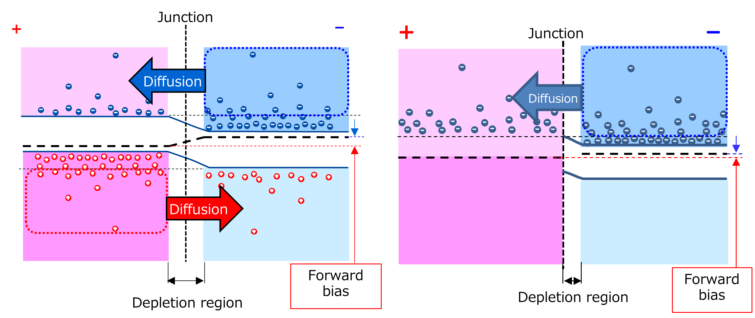
When forward-biased, pn junction diodes turn on as electrons, minority carriers, flow into the p-type semiconductor while holes flow into the n-type semiconductor. Since both electrons and holes contribute to device operation, pn junction diodes are called bipolar devices. On the other hand, in the case of an SBD composed of an n-type semiconductor and a metal, majority carriers flow into the metal when the SBD is forward-biased, causing it to turn on. Since only majority carriers contribute to device operation, SBDs are called unipolar devices.
Bipolar type diodes, such as p-n junction diodes, have a low concentration N-layer to increase the device's breakdown voltage. This layer acts as a resistor when turned on, which has the disadvantage of increasing forward voltage. However, in actual operation when turned on, a large amount of holes flow from the P+ layer on the anode side into the N- layer. At the same time, a large amount of electrons are supplied from the cathode side to maintain electrical neutrality. As a result, a large number of carriers temporarily exist in the N- layer, resulting in a low resistance value. This is called conductivity modulation.
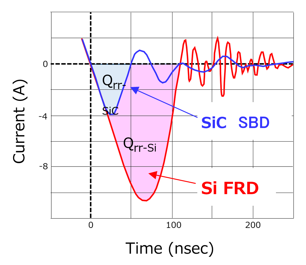
This is good in terms of lowering the on-voltage (forward voltage) of the device, but it also has the disadvantage that it cannot be turned off immediately (it takes time to turn off). This is because a large number of minority carriers (holes) that have entered the N-layer due to conductivity modulation have nowhere to go, and it takes time for these excess minority carriers to disappear through recombination. This period is called the reverse recovery time, and a reverse current flows. In contrast, in the case of SDBs, the minority carriers of the n-type (or p-type) semiconductor do not contribute to device operation. Therefore, SBDs exhibit no reverse recovery time. However, considerable surface leakage occurs since SBDs consist of a heterogeneous junction between a metal and a semiconductor. In some SBDs, a pn junction is sometimes used to reduce this leakage. In addition to this, it has parasitic capacitance, so it may have a reverse recovery time, although it is minute compared to a pn junction diode.
Conductivity modulation is explained in the e-learning below. please refer.
e-learning:Basics of Schottky Barrier Diodes 2-3. Conductivity modulation
Related Links
FAQs
The following documents also contain related information.


Company names, product names, and service names used in this FAQ may be of their respective companies.