
- General Top
- SEMICONDUCTOR
- STORAGE
- COMPANY
-
My ToshibaSemicon
- Semiconductor Top
-
ApplicationsAutomotive
Body Electronics
xEV
In-Vehicle Infotainment
Advanced Driver-Assistance Systems (ADAS)
Chassis
IndustrialInfrastructure
BEMS/HEMS
Factory Automation
Commercial Equipment
Consumer/PersonalIoT Equipment
Healthcare
Wearable Device
Mobile
Computer Peripherals
-
ProductsAutomotive Devices
Discrete Semiconductor
Diodes
Transistors
Logic ICs
Analog Devices
Digital Devices
Wireless Devices
※
 : Products list (parametric search)Power Semiconductors
SiC Power Devices
※
: Products list (parametric search)Isolators/Solid State RelaysPhotocouplers
Digital Isolators
Solid State Relays
Fiber Optic Transmitting Modules
※
: Products list (parametric search)MOSFETsIGBTs/IEGTsBipolar Transistors※
: Products list (parametric search)Diodes※
: Products list (parametric search)MicrocontrollersMotor Driver ICsIntelligent Power ICs※
: Products list (parametric search)Power Management ICsLinear ICs※
: Products list (parametric search)General Purpose Logic ICsLinear Image SensorsOther Product ICsOther Product ICs
※
: Products list (parametric search) -
Design & Development
-
Knowledge
- Where To Buy


- Part Number & Keyword Search
- Cross Reference Search
- Parametric Search
- Stock Check & Purchase
This webpage doesn't work with Internet Explorer. Please use the latest version of Google Chrome, Microsoft Edge, Mozilla Firefox or Safari.
require 3 characters or more. Search for multiple part numbers fromhere.
The information presented in this cross reference is based on TOSHIBA's selection criteria and should be treated as a suggestion only. Please carefully review the latest versions of all relevant information on the TOSHIBA products, including without limitation data sheets and validate all operating parameters of the TOSHIBA products to ensure that the suggested TOSHIBA products are truly compatible with your design and application.Please note that this cross reference is based on TOSHIBA's estimate of compatibility with other manufacturers' products, based on other manufacturers' published data, at the time the data was collected.TOSHIBA is not responsible for any incorrect or incomplete information. Information is subject to change at any time without notice.
require 3 characters or more.
How are super-junction MOSFETs different from common D-MOS?
The depletion layer spreads differently in N-layer, which determines the limit of the breakdown voltage. SJ-MOS can be designed with N-layers with lower resistivity, allowing for lower on-resistance.
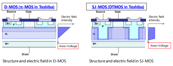
SJ-MOS (we call it DTMOS) forms a columnar P layer (P-pillar layer) on a part of N-layer and alternates P-N layers.
When VDS is applied, the depletion layer spreads over N-layer, which is the drifting layer. However, the spreads differently in the common D-MOS (called π-MOS in our case) and SJ-MOS. (See the electric field intensity diagram. The electric field intensity indicates the state in the depletion layer.)
In D-MOS, the interface between P/N-layers has the highest electric field strength, and breakover (breakdown phenomena) occurs when this part exceeds the limit of the material-silicon. This is the limit of the breakdown voltage. On the other hand, SJ-MOS has uniform electric field strength in N-layers.
As a consequence, SJ-MOS can be designed with lower-resistance N-layers, allowing for lower on-resistance.
Please also refer to FAQ below.