
- General Top
- SEMICONDUCTOR
- STORAGE
- COMPANY
-
My ToshibaSemicon
- Semiconductor Top
-
ApplicationsAutomotive
Body Electronics
xEV
In-Vehicle Infotainment
Advanced Driver-Assistance Systems (ADAS)
Chassis
IndustrialInfrastructure
BEMS/HEMS
Factory Automation
Commercial Equipment
Consumer/PersonalIoT Equipment
Healthcare
Wearable Device
Mobile
Computer Peripherals
-
ProductsAutomotive Devices
Discrete Semiconductor
Diodes
Transistors
Logic ICs
Analog Devices
Digital Devices
Wireless Devices
※
 : Products list (parametric search)Power Semiconductors
SiC Power Devices
※
: Products list (parametric search)Isolators/Solid State RelaysPhotocouplers
Digital Isolators
Solid State Relays
Fiber Optic Transmitting Modules
※
: Products list (parametric search)MOSFETsIGBTs/IEGTsBipolar Transistors※
: Products list (parametric search)Diodes※
: Products list (parametric search)MicrocontrollersMotor Driver ICsIntelligent Power ICs※
: Products list (parametric search)Power Management ICsLinear ICs※
: Products list (parametric search)General Purpose Logic ICsLinear Image SensorsOther Product ICsOther Product ICs
※
: Products list (parametric search) -
Design & Development
-
Knowledge
- Where To Buy


- Part Number & Keyword Search
- Cross Reference Search
- Parametric Search
- Stock Check & Purchase
This webpage doesn't work with Internet Explorer. Please use the latest version of Google Chrome, Microsoft Edge, Mozilla Firefox or Safari.
require 3 characters or more. Search for multiple part numbers fromhere.
The information presented in this cross reference is based on TOSHIBA's selection criteria and should be treated as a suggestion only. Please carefully review the latest versions of all relevant information on the TOSHIBA products, including without limitation data sheets and validate all operating parameters of the TOSHIBA products to ensure that the suggested TOSHIBA products are truly compatible with your design and application.Please note that this cross reference is based on TOSHIBA's estimate of compatibility with other manufacturers' products, based on other manufacturers' published data, at the time the data was collected.TOSHIBA is not responsible for any incorrect or incomplete information. Information is subject to change at any time without notice.
require 3 characters or more.
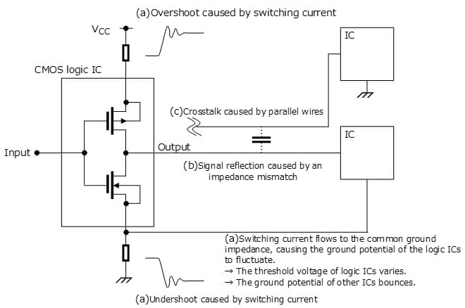
Input Rise and Fall Time Specifications
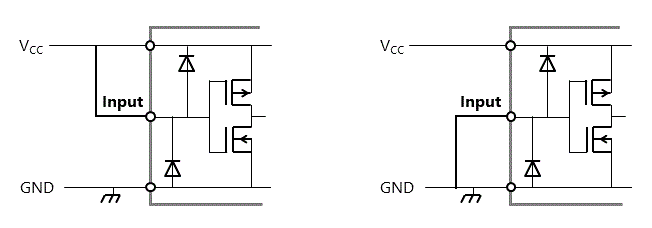
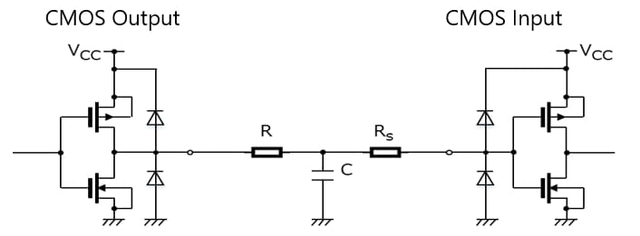
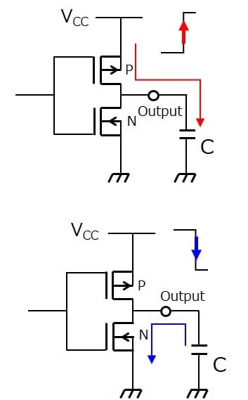
In the datasheet, the input rise and fall times of general-purpose CMOS logic ICs are specified in the operating ranges in which their functional operation is guaranteed.
Use CMOS logic ICs within the operating ranges to prevent a malfunction due to output oscillation etc.
If a slowly rising or falling signal (a low slew rate signal) is applied to an input, a current spike occurs during switching, causing VCC and GND bounce, which might result in output oscillation or a malfunction.
Use ICs with a Schmitt-trigger input for slowly changing inputs. However, in the case of excessively slowly changing inputs, even ICs with a Schmitt-trigger input might not be able to suppress noise on power supply or signal lines, resulting in output oscillation or instability.
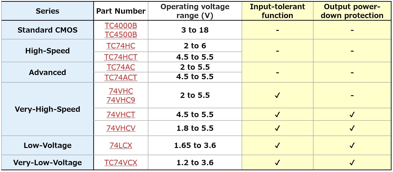
The following table shows the rise and fall times of a typical IC*1 in each series.
| Type | Series Name | Series No. | One-Gate Logic (L-MOS) Equivalents | Operating Voltage Range (V) | Propagation Delay Times*1, tpLH and tpHL (ns) | Output Current*2, IOUT (mA) | Rise and Fall Times at 3.3 V | Rise and Fall Times at 5 V |
|---|---|---|---|---|---|---|---|---|
For 5-V Systems |
Standard | TC40xxB TC45xxB |
TC4S TC4W |
3 to 18 | 200 (at 5.0 V) |
±0.51 (at 5.0 V) |
0 to 10000 ns *6 | 0 to 5000 ns *6 |
| High Speed | TC74HC | TC7S TC7W |
2 to 6 | 23 (at 4.5 V) |
±4.0 or 6.0 (at 4.5 V) (±2.0 in the case of TC7S) |
0 to 1000 ns at 2 V |
0 to 500 ns at 4.5 V |
|
| TC74HCT | TC7WT | 4.5 to 5.5 | 28 (at 4.5 V) |
- | 0 to 500 ns | |||
Advanced |
TC74AC | - | 2 to 5.5 | 8.5 (at 4.5 V) |
±24 (at 4.5 V) |
0 to 100 ns/V | 0 to 20 ns/V | |
| TC74ACT | - | 4.5 to 5.5 | 9.0 (at 5.0 V) |
- | 0 to 10 ns/V | |||
Very High Speed |
TC74VHC 74VHC |
TC7SH TC7WH |
2 to 5.5 | 8.5 (at 5.0 V) |
±8.0 (at 4.5 V) |
0 to 100 ns/V | 0 to 20 ns/V | |
| TC74VHC9 74VHC9 |
10 (at 5.0 V) |
- *5 | - *5 | |||||
| TC74VHCT 74VHCT |
TC7SET | 4.5 to 5.5 | 9.5 (at 5.0 V) |
- | 0 to 20 ns/V | |||
| TC74VHCV 74VHCV |
- | 1.8 to 5.5 | 8.5 (at 5.0 V) |
±16 (at 4.5 V) |
0 to 20 ms/V | 0 to 1 ms/V | ||
For low-voltage systems |
Medium Speed | TC74LCX 74LCX |
TC7SZ TC7PZ TC7WZ |
1.65 to 3.6 (1.65 to 5.5 in the case of TC7SZ/PZ/WZ) |
6.5 (at 5.0 V) |
±24 (at 3.0 V) |
0 to 10 ns/V | - |
| High Speed | TC74VCX | 7UL | 1.2 to 3.6 (0.9 to 3.6 in the case of 7UL) |
4.2 (at 2.3 V) |
±24 (at 3.0 V) (±8.0 in the case of 7UL) |
0 to 10 ns/V | - |
*1: Maximum propagation delay time of typical ICs (TC4001, TC74HC244, TC74AC244, TC74VHC244, TC74LCX244, and TC74VCX244) at 85°C, except for the TC4001 for which the maximum propagation delay time at 25°C is shown
*2: Output current values are specified in the DC Characteristics table shown in the datasheet. Absolute maximum rated output current is specified separately.
*3: The TC7SET series does not have an output power-down protection function.
*4: The ICs of the TC7SZ series in the fSV package do not have an output power-down protection function except those with an open-drain output.
*5: Rise and fall times are not specified because the TC74VHC9 and 74VHC9 series provide Schmitt-trigger inputs.
*6: Rise and fall times are not specified in the datasheet. The values shown above should be considered only as a guide for creating a design.
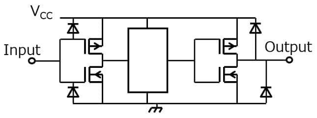
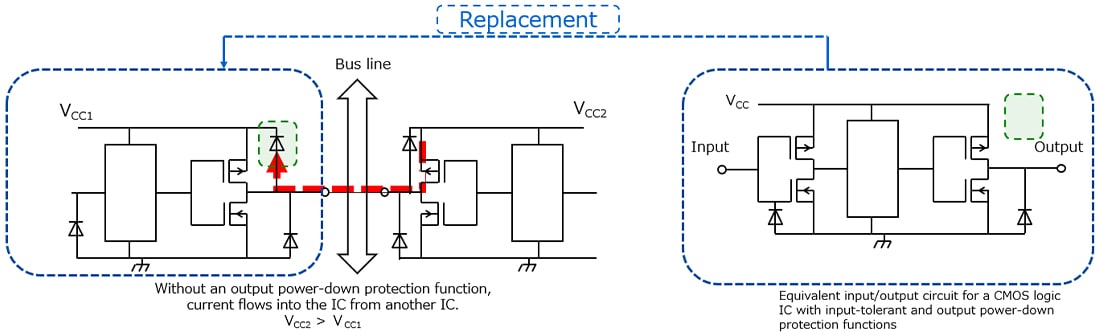
Usage Considerations of CMOS Logic ICs

Products
Related information
- Application Notes
- FAQ