
- General Top
- SEMICONDUCTOR
- STORAGE
- COMPANY
-
My ToshibaSemicon
- Semiconductor Top
-
ApplicationsAutomotive
Body Electronics
xEV
In-Vehicle Infotainment
Advanced Driver-Assistance Systems (ADAS)
Chassis
IndustrialInfrastructure
BEMS/HEMS
Factory Automation
Commercial Equipment
Consumer/PersonalIoT Equipment
Healthcare
Wearable Device
Mobile
Computer Peripherals
-
ProductsAutomotive Devices
Discrete Semiconductor
Diodes
Transistors
Logic ICs
Analog Devices
- Automotive SmartMCD™ (Integreted SoC Conbining Microcontroller and Driver)
- Automotive Brushless Motor Driver ICs
- Automotive Brushed DC Motor Driver ICs
- Automotive Stepping Motor Driver ICs
- Automotive Driver ICs
- Automotive System Power Supplies ICs
- Automotive audio power amplifier ICs
- Automotive Network Communication
Digital Devices
Wireless Devices
※
 : Products list (parametric search)Power Semiconductors
SiC Power Devices
※
: Products list (parametric search)Isolators/Solid State RelaysPhotocouplers
Digital Isolators
Solid State Relays
Fiber Optic Transmitting Modules
※
: Products list (parametric search)MOSFETsIGBTs/IEGTsBipolar Transistors※
: Products list (parametric search)Diodes※
: Products list (parametric search)MicrocontrollersMotor Driver ICsIntelligent Power ICs※
: Products list (parametric search)Power Management ICsLinear ICs※
: Products list (parametric search)General Purpose Logic ICsLinear Image SensorsOther Product ICsOther Product ICs
※
: Products list (parametric search) -
Design & Development
-
Knowledge
- Where To Buy


- Part Number & Keyword Search
- Cross Reference Search
- Parametric Search
- Stock Check & Purchase
This webpage doesn't work with Internet Explorer. Please use the latest version of Google Chrome, Microsoft Edge, Mozilla Firefox or Safari.
require 3 characters or more. Search for multiple part numbers fromhere.
The information presented in this cross reference is based on TOSHIBA's selection criteria and should be treated as a suggestion only. Please carefully review the latest versions of all relevant information on the TOSHIBA products, including without limitation data sheets and validate all operating parameters of the TOSHIBA products to ensure that the suggested TOSHIBA products are truly compatible with your design and application.Please note that this cross reference is based on TOSHIBA's estimate of compatibility with other manufacturers' products, based on other manufacturers' published data, at the time the data was collected.TOSHIBA is not responsible for any incorrect or incomplete information. Information is subject to change at any time without notice.
require 3 characters or more.
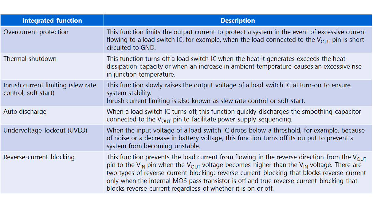
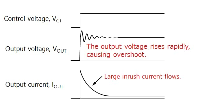
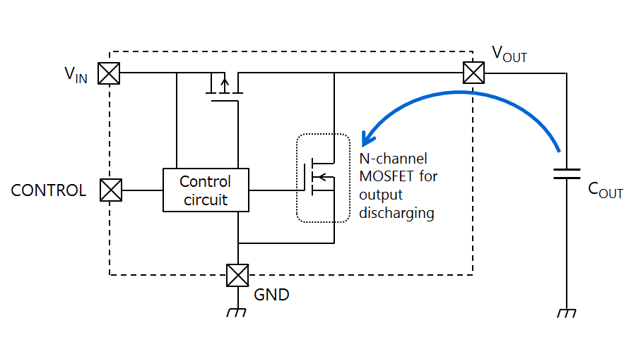
2-7. Reverse-current protection
The reverse-current blocking circuit blocks the current flowing in the reverse direction from the VOUT pin to the VIN pin when output voltage (VOUT) > input voltage (VIN).
Toshiba’s load switch ICs are available with two types of reverse-current blocking circuit:
a) Reverse-current blocking activated only when a load switch IC is off
When the MOS pass transistor turns off, VIN becomes lower than VOUT to prevent reverse current from flowing from the VOUT pin to the VIN pin. Reverse-current blocking is disabled while the MOS pass transistor is on.
b) True reverse-current blocking
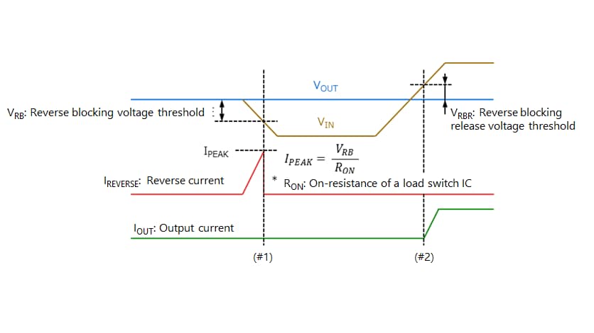
A true reverse-current blocking function prevents reverse current from flowing from the VOUT pin to the VIN pin regardless of whether the MOS pass transistor is on or off. The reverse-current blocking circuit is enabled when VOUT becomes higher than VIN by VRB (reverse blocking voltage threshold) and is disabled when VOUT becomes lower than VIN by VRBR (reverse blocking release voltage threshold).

The following figure shows the reverse-current characteristics of a load switch IC with a true reverse-current blocking function. As highlighted by the red line (#1), IREVERSE increases as the difference between VOUT and VIN (VOUT – VIN) increases. Reverse-current blocking is enabled when VOUT – VIN reaches Point A at which it is approximately 40 mV, blocking IREVERSE. When VIN becomes higher than VOUT by roughly 30 mV (at Point B) as highlighted by the green line (#2), reverse-current blocking is disabled, causing current to begin flowing again from the VIN pin to the VOUT pin.
Chapter2 Convenient functions load switch ICs

Related information
- Products
Load Switch ICs - Applidcation Notes
Application Notes - FAQs
Load Switch ICs - Parametric Search
Parametric search - Stock Check & Purchase
Stock Check & Purchase