


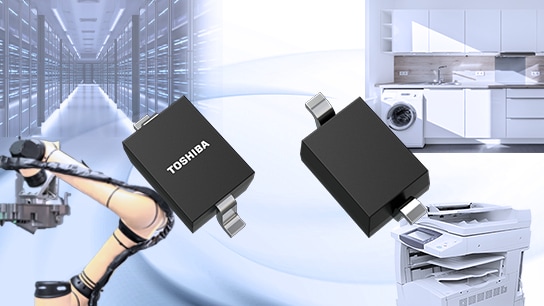
Zener Diodes
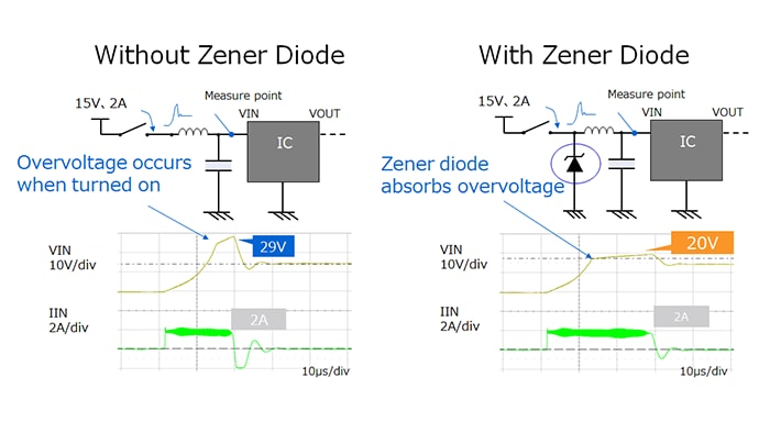
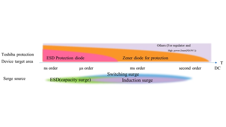
A Zener diode is characterized by its ability to protect an object from transient overvoltage pulses as well as overvoltage pulses close to DC, which are difficult to protect against with ESD protection diodes.
In equipment power lines, switching surges with long pulse widths up to milliseconds may be generated when the circuit switches. Zener diodes protect semiconductor devices from switching surges and overvoltage with a frequency close to DC. It can also protect semiconductor devices from ESD[2] with a width of several hundred nanoseconds and inductive lightning surges[1] with a pulse width in the order of microseconds as well. This contributes toward improved equipment reliability.
Zener diodes are available in a wide range of Zener voltage specifications extending from 5.6 V to 82 V. Their extensive application fields include both consumer and industrial electronics.
[1] @IEC61000-4-5, tp=8/20 μs
[2] @IEC61000-4-2
Lineup
You can narrow down the search for applicable products by selecting specifications.
You can narrow down your search for applicable products by package type or number of pins.

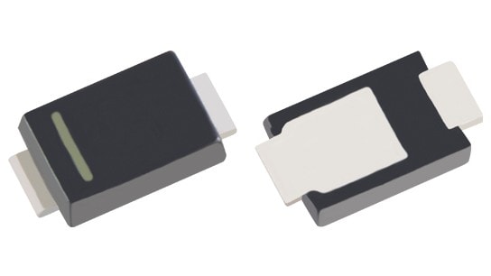
- SOD-962 (SL2)
-
Package Size
W : 0.62 mm 0.024 inch L : 0.32 mm 0.013 inch H : 0.3 mm 0.012 inch

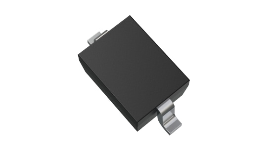
- SOD-882 (CST2)
-
Package Size
W : 1.0 mm 0.039 inch L : 0.6 mm 0.024 inch H : 0.38 mm 0.015 inch

- SOD-523 (ESC)
-
Package Size
W : 1.6 mm 0.063 inch L : 0.8 mm 0.031 inch H : 0.6 mm 0.024 inch

- SOD-323 (USC)
-
Package Size
W : 2.5 mm 0.098 inch L : 1.25 mm 0.049 inch H : 0.9 mm 0.035 inch

- SOD-323HE (US2H)
-
Package Size
W : 2.5 mm 0.098 inch L : 1.4 mm 0.055 inch H : 0.60 mm 0.024 inch

- S-FLAT
-
Package Size
W : 1.6 mm 0.063 inch L : 3.5 mm 0.14 inch H : 0.98 mm 0.039 inch

- M-FLAT
-
Package Size
W : 2.4 mm 0.094 inch L : 4.7 mm 0.19 inch H : 0.98 mm 0.039 inch

- SOT-323 (USM)
-
Package Size
W : 2.0 mm 0.079 inch L : 2.1 mm 0.083 inch H : 0.9 mm 0.035 inch

- SOT-23 (SOT23)
-
Package Size
W : 2.9 mm 0.11 inch L : 2.4 mm 0.094 inch H : 0.9 mm 0.035 inch

- SOT-346 (S-Mini)
-
Package Size
W : 2.9 mm 0.11 inch L : 2.5 mm 0.098 inch H : 1.1 mm 0.043 inch
All package dimensions are guaranteed in millimeters as mentioned on datasheet. Package dimension in inches is round to 2 significant digits converted with 1mm=0.0393701inch.
require 3 characters or more.
About information presented in this cross reference
The information presented in this cross reference is based on TOSHIBA's selection criteria and should be treated as a suggestion only. Please carefully review the latest versions of all relevant information on the TOSHIBA products, including without limitation data sheets and validate all operating parameters of the TOSHIBA products to ensure that the suggested TOSHIBA products are truly compatible with your design and application.Please note that this cross reference is based on TOSHIBA's estimate of compatibility with other manufacturers' products, based on other manufacturers' published data, at the time the data was collected.TOSHIBA is not responsible for any incorrect or incomplete information. Information is subject to change at any time without notice.


Documents
Applications


Reference Design
Queries about purchasing, sampling and IC reliability
Stock Check & Purchase
require 3 characters or more.
Through this website you are able to proceed to the website of our distributors ("Third Party Website") which is not under the control of Toshiba Corporation and its subsidiaries and affiliates (collectively "Toshiba"). The Third Party Website is made available to you as a convenience only and you agree to use the Third Party Website at your own risk. The link of the Third Party Website does not necessarily imply a recommendation or an endorsement by Toshiba of the Third Party Website. Please be aware that Toshiba is not responsible for any transaction done through the Third Party Website, and such transactions shall be subject to terms and conditions which may be provided in the Third Party Website.