
- General Top
- SEMICONDUCTOR
- STORAGE
- COMPANY
-
My ToshibaSemicon
- Semiconductor Top
-
ApplicationsAutomotive
Body Electronics
xEV
In-Vehicle Infotainment
Advanced Driver-Assistance Systems (ADAS)
Chassis
IndustrialInfrastructure
BEMS/HEMS
Factory Automation
Commercial Equipment
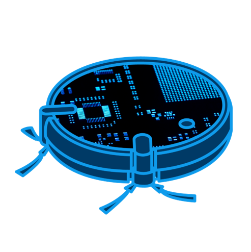
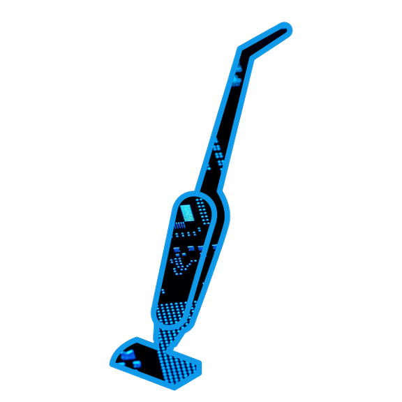
Consumer/PersonalIoT Equipment
Healthcare
Wearable Device
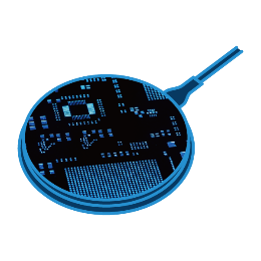
Mobile
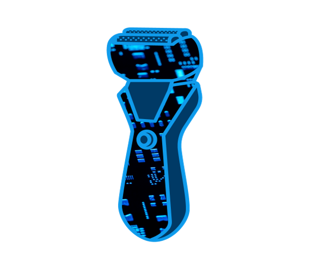
Computer Peripherals
-
ProductsAutomotive Devices
Discrete Semiconductor
Diodes
Transistors
Logic ICs
Analog Devices
- Automotive SmartMCD™ (Integreted SoC Conbining Microcontroller and Driver)
- Automotive Brushless Motor Driver ICs
- Automotive Brushed DC Motor Driver ICs
- Automotive Stepping Motor Driver ICs
- Automotive Driver ICs
- Automotive System Power Supplies ICs
- Automotive audio power amplifier ICs
- Automotive Network Communication
Digital Devices
Wireless Devices
※
 : Products list (parametric search)Power Semiconductors
SiC Power Devices
※
: Products list (parametric search)Isolators/Solid State RelaysPhotocouplers
Digital Isolators
Solid State Relays
Fiber Optic Transmitting Modules
※
: Products list (parametric search)MOSFETs- 12V - 300V MOSFETs
- 400V - 900V MOSFETs
- Automotive MOSFETs
- MOSFET Gate Driver ICs
- SiC MOSFETs
- SiC MOSFET Modules
IGBTs/IEGTsBipolar Transistors※
: Products list (parametric search)Diodes※
: Products list (parametric search)MicrocontrollersMotor Driver ICsIntelligent Power ICs※
: Products list (parametric search)Power Management ICs- LDO Regulators
- Load Switch ICs
- eFuse ICs
- MOSFET Gate Driver ICs
- PFC Control ICs
- LED Driver ICs
Linear ICs※
: Products list (parametric search)General Purpose Logic ICsLinear Image SensorsOther Product ICsOther Product ICs
※
: Products list (parametric search) -
Design & Development
-
Knowledge
- Where To Buy


- Part Number & Keyword Search
- Cross Reference Search
- Parametric Search
- Stock Check & Purchase
This webpage doesn't work with Internet Explorer. Please use the latest version of Google Chrome, Microsoft Edge, Mozilla Firefox or Safari.
require 3 characters or more. Search for multiple part numbers fromhere.
The information presented in this cross reference is based on TOSHIBA's selection criteria and should be treated as a suggestion only. Please carefully review the latest versions of all relevant information on the TOSHIBA products, including without limitation data sheets and validate all operating parameters of the TOSHIBA products to ensure that the suggested TOSHIBA products are truly compatible with your design and application.Please note that this cross reference is based on TOSHIBA's estimate of compatibility with other manufacturers' products, based on other manufacturers' published data, at the time the data was collected.TOSHIBA is not responsible for any incorrect or incomplete information. Information is subject to change at any time without notice.
require 3 characters or more.
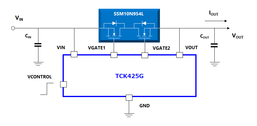
MOSFET Gate Driver ICs
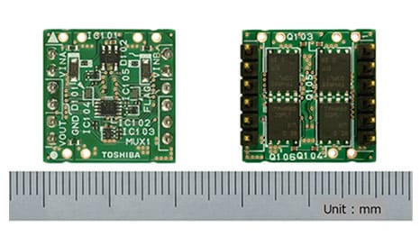
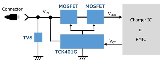
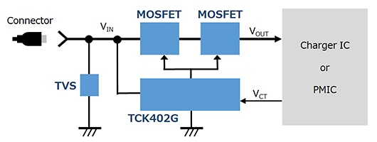
Toshiba MOSFET Gate Driver IC is an ON and Off switching control device for external N-channel MOSFET. Toshiba MOSFET Gate Driver ICs have charge pump and protection circuits and they feature ultra small package (1.2x0.8 mm), low quiescent current and wide input voltage. Using them with Toshiba MOSFET, Toshiba suppor various technical data such as simlation, switching evaluation and SOA (Safe Operating Area).
Lineup
You can narrow down the search for applicable products by selecting specifications.
You can narrow down your search for applicable products by package type or number of pins.
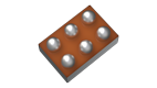
- WCSP6E
-
Package Size
W : 1.2 mm 0.047 inch L : 0.8 mm 0.031 inch H : 0.55 mm 0.022 inch
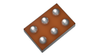
- WCSP6G
-
Package Size
W : 1.2 mm 0.047 inch L : 0.8 mm 0.031 inch H : 0.35 mm 0.014 inch
All package dimensions are guaranteed in millimeters as mentioned on datasheet. Package dimension in inches is round to 2 significant digits converted with 1mm=0.0393701inch.
require 3 characters or more.
About information presented in this cross reference
The information presented in this cross reference is based on TOSHIBA's selection criteria and should be treated as a suggestion only. Please carefully review the latest versions of all relevant information on the TOSHIBA products, including without limitation data sheets and validate all operating parameters of the TOSHIBA products to ensure that the suggested TOSHIBA products are truly compatible with your design and application.Please note that this cross reference is based on TOSHIBA's estimate of compatibility with other manufacturers' products, based on other manufacturers' published data, at the time the data was collected.TOSHIBA is not responsible for any incorrect or incomplete information. Information is subject to change at any time without notice.
Technical Articles

MOSFET Gate Driver ICs
Documents
Applications

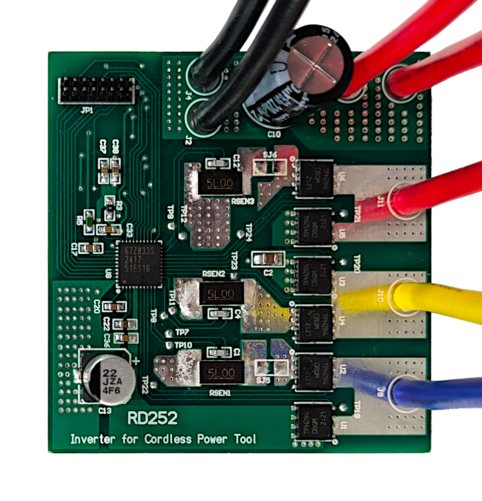
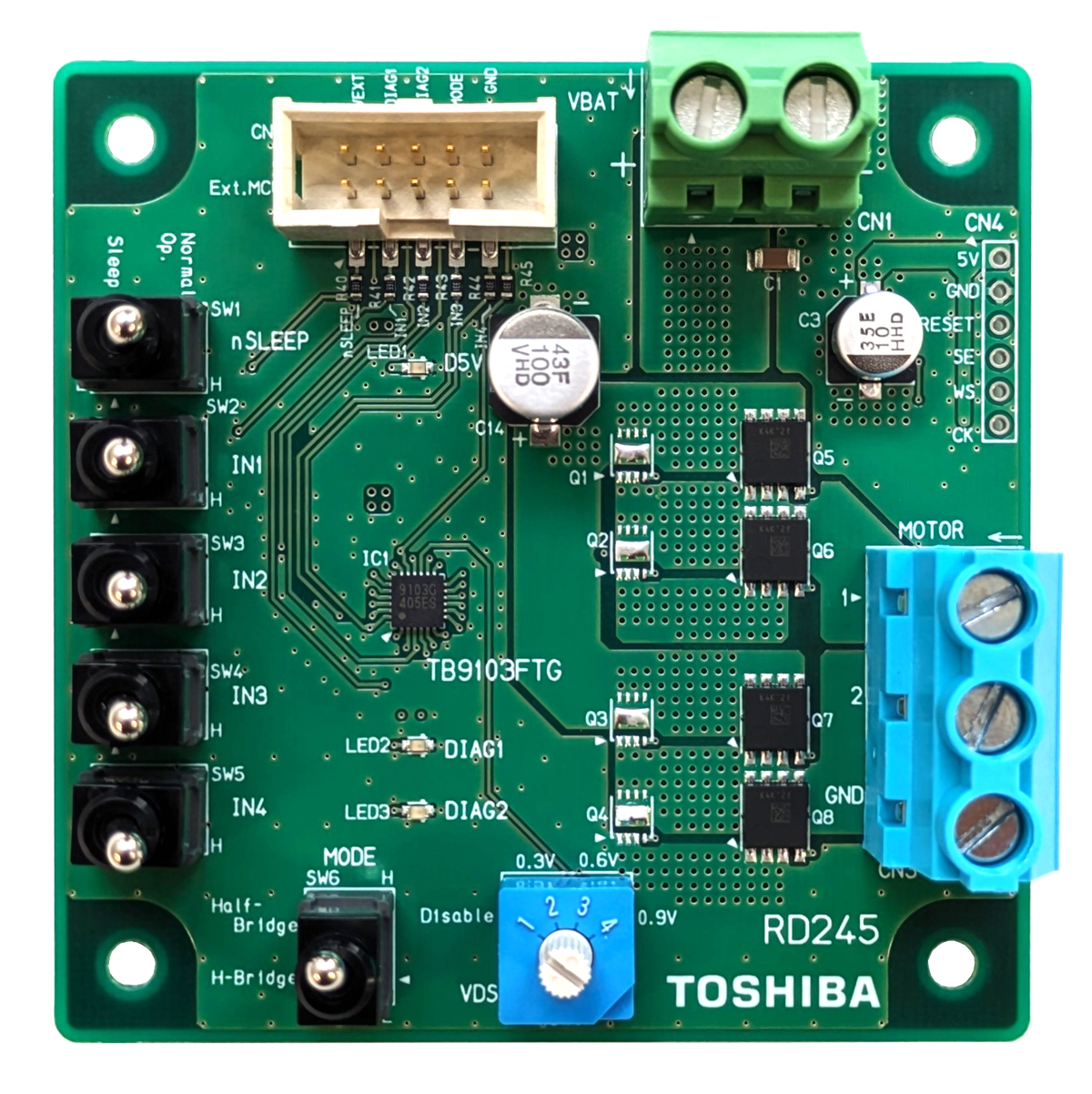
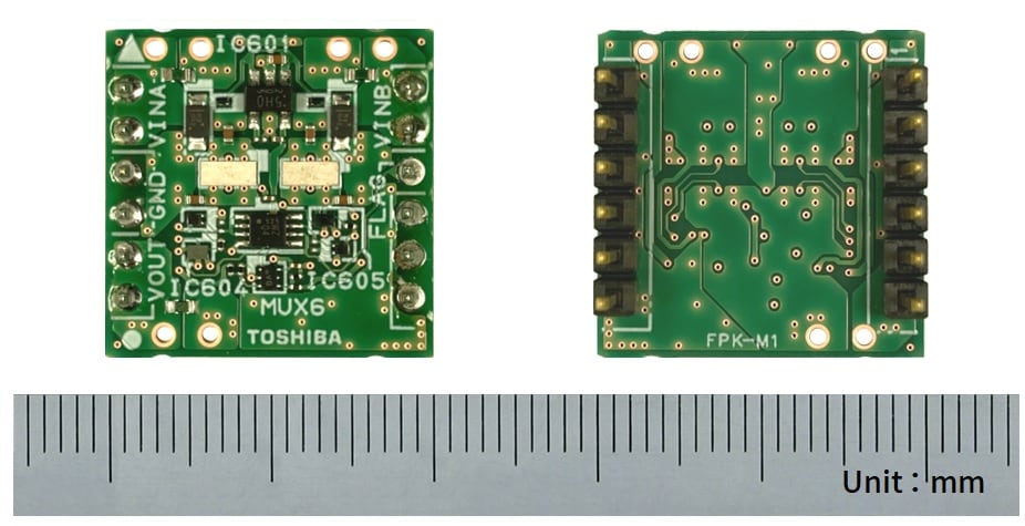
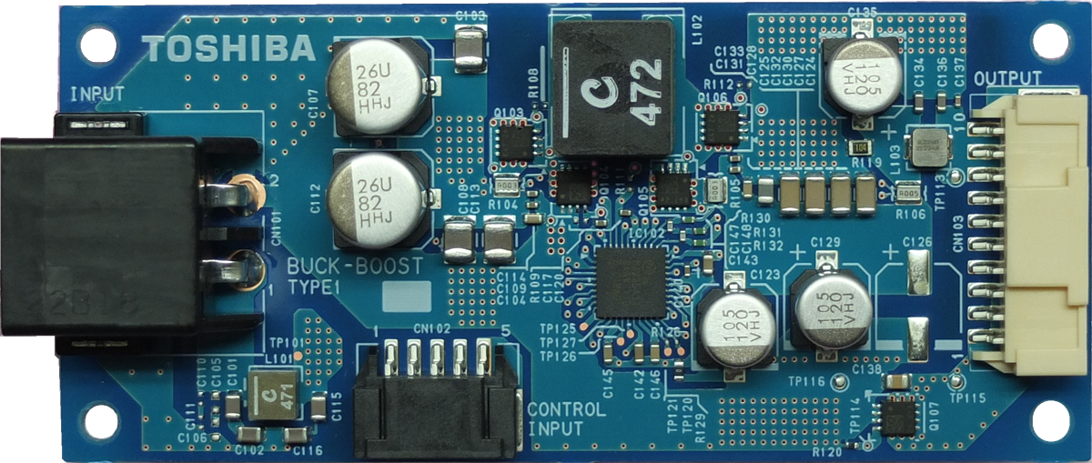
Reference Design
Queries about purchasing, sampling and IC reliability
Stock Check & Purchase
require 3 characters or more.
Through this website you are able to proceed to the website of our distributors ("Third Party Website") which is not under the control of Toshiba Corporation and its subsidiaries and affiliates (collectively "Toshiba"). The Third Party Website is made available to you as a convenience only and you agree to use the Third Party Website at your own risk. The link of the Third Party Website does not necessarily imply a recommendation or an endorsement by Toshiba of the Third Party Website. Please be aware that Toshiba is not responsible for any transaction done through the Third Party Website, and such transactions shall be subject to terms and conditions which may be provided in the Third Party Website.