
- General Top
- SEMICONDUCTOR
- STORAGE
- COMPANY
-
My ToshibaSemicon
- Semiconductor Top
-
ApplicationsAutomotive
Body Electronics
xEV
In-Vehicle Infotainment
Advanced Driver-Assistance Systems (ADAS)
Chassis
IndustrialInfrastructure
BEMS/HEMS
Factory Automation
Commercial Equipment
Consumer/PersonalIoT Equipment
Healthcare
Wearable Device
Mobile
Computer Peripherals
-
ProductsAutomotive Devices
Discrete Semiconductor
Diodes
Transistors
Logic ICs
Analog Devices
- Automotive SmartMCD™ (Integreted SoC Conbining Microcontroller and Driver)
- Automotive Brushless Motor Driver ICs
- Automotive Brushed DC Motor Driver ICs
- Automotive Stepping Motor Driver ICs
- Automotive Driver ICs
- Automotive System Power Supplies ICs
- Automotive audio power amplifier ICs
- Automotive Network Communication
Digital Devices
Wireless Devices
※
 : Products list (parametric search)Power Semiconductors
SiC Power Devices
※
: Products list (parametric search)Isolators/Solid State RelaysPhotocouplers
Digital Isolators
Solid State Relays
Fiber Optic Transmitting Modules
※
: Products list (parametric search)MOSFETsIGBTs/IEGTsBipolar Transistors※
: Products list (parametric search)Diodes※
: Products list (parametric search)MicrocontrollersMotor Driver ICsIntelligent Power ICs※
: Products list (parametric search)Power Management ICsLinear ICs※
: Products list (parametric search)General Purpose Logic ICsLinear Image SensorsOther Product ICsOther Product ICs
※
: Products list (parametric search) -
Design & Development
-
Knowledge
- Where To Buy


- Part Number & Keyword Search
- Cross Reference Search
- Parametric Search
- Stock Check & Purchase
This webpage doesn't work with Internet Explorer. Please use the latest version of Google Chrome, Microsoft Edge, Mozilla Firefox or Safari.
require 3 characters or more. Search for multiple part numbers fromhere.
The information presented in this cross reference is based on TOSHIBA's selection criteria and should be treated as a suggestion only. Please carefully review the latest versions of all relevant information on the TOSHIBA products, including without limitation data sheets and validate all operating parameters of the TOSHIBA products to ensure that the suggested TOSHIBA products are truly compatible with your design and application.Please note that this cross reference is based on TOSHIBA's estimate of compatibility with other manufacturers' products, based on other manufacturers' published data, at the time the data was collected.TOSHIBA is not responsible for any incorrect or incomplete information. Information is subject to change at any time without notice.
require 3 characters or more.
3-5. Reverse recovery time
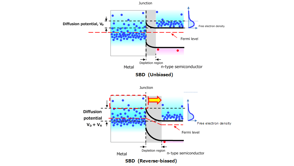
When diodes and other semiconductor devices are on, current flows because of free electrons and holes (carriers). In addition, these carriers are accumulated as electric charge in the depletion region formed across a junction or in a parasitic capacitor and also accumulated in the lightly doped region as excess carriers. (This causes the above-mentioned conductivity modulation.) When these devices transition from the on state to the off state, they release electrons just like a capacitor. The resulting flow of electrons is observed as a current flow in the opposite direction.
The forward voltage (VF) is positive while the current (iF) is between zero and the peak reverse recovery current (Irr). During this period, the electric charge in the depletion region and the parasitic capacitor is mainly released, causing negative current to flow. Once iF reaches Irr, the excessive carriers (electrons and holes) that contributed to the conductivity modulation disappear because they recombine. Therefore, the time required for this recombination depends on the carrier lifetime.
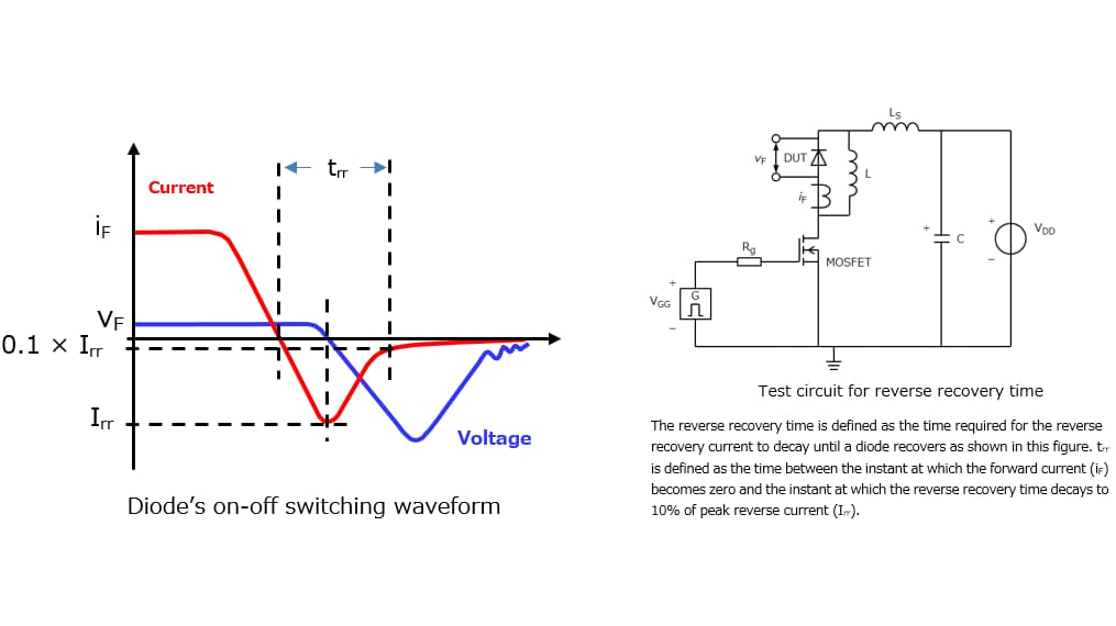
As described above, conductivity modulation occurs in bipolar devices such as pn junction diodes whereas theoretically it does not occur in unipolar devices such as SBDs. Therefore, SBDs exhibit almost zero reverse recovery time.
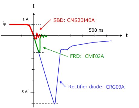
Figure 3-9 compares the reverse recovery characteristics of two typical pn junction diodes—the CRG09A rectifier diode (VR=400 V, IF=1 A) and the CMF02A fast recovery diode (VR=600 V, IF=1 A)—with the CMS20I40A SBD (VR=40 V, IF=2 A). Although it is difficult to make simple comparisons because their maximum rated reverse voltages are different, the reverse recovery time of the fast recovery diode (FRD) is much smaller than that of the rectifier diode whereas the reverse recovery time of the SBD is nearly zero.
Chapter3 Basics of Schottky Barrier Diodes

Related information
- Products
Schottky Barrier Diodes - Application Notes
Application Notes - FAQs
Diodes - Parametric Search
Schottky Barrier Diodes - Stock Check & Purchase
Stock Check & Purchase