- General Top
- SEMICONDUCTOR
- STORAGE
- COMPANY
-
My ToshibaSemicon
- Semiconductor Top
-
ApplicationsAutomotive
Body Electronics
xEV
In-Vehicle Infotainment
Advanced Driver-Assistance Systems (ADAS)
Chassis
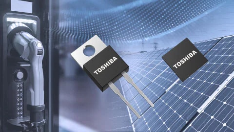
IndustrialInfrastructure
BEMS/HEMS
Factory Automation
Commercial Equipment
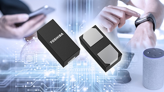
Consumer/PersonalIoT Equipment
Healthcare
Wearable Device
Mobile
Computer Peripherals
-
ProductsAutomotive Devices
Discrete Semiconductor
Diodes
Transistors
Logic ICs
Analog Devices
- Automotive SmartMCD™ (Integreted SoC Conbining Microcontroller and Driver)
- Automotive Brushless Motor Driver ICs
- Automotive Brushed DC Motor Driver ICs
- Automotive Stepping Motor Driver ICs
- Automotive Driver ICs
- Automotive System Power Supplies ICs
- Automotive audio power amplifier ICs
- Automotive Network Communication
Digital Devices
Wireless Devices
※
 : Products list (parametric search)Power Semiconductors
SiC Power Devices
※
: Products list (parametric search)Isolators/Solid State RelaysPhotocouplers
Digital Isolators
Solid State Relays
Fiber Optic Transmitting Modules
※
: Products list (parametric search)MOSFETsIGBTs/IEGTsBipolar Transistors※
: Products list (parametric search)Diodes※
: Products list (parametric search)MicrocontrollersMotor Driver ICsIntelligent Power ICs※
: Products list (parametric search)Power Management ICsLinear ICs※
: Products list (parametric search)General Purpose Logic ICsLinear Image SensorsOther Product ICsOther Product ICs
※
: Products list (parametric search) -
Design & Development
-
Knowledge
- Where To Buy


- Part Number & Keyword Search
- Cross Reference Search
- Parametric Search
- Stock Check & Purchase
This webpage doesn't work with Internet Explorer. Please use the latest version of Google Chrome, Microsoft Edge, Mozilla Firefox or Safari.
require 3 characters or more. Search for multiple part numbers fromhere.
The information presented in this cross reference is based on TOSHIBA's selection criteria and should be treated as a suggestion only. Please carefully review the latest versions of all relevant information on the TOSHIBA products, including without limitation data sheets and validate all operating parameters of the TOSHIBA products to ensure that the suggested TOSHIBA products are truly compatible with your design and application.Please note that this cross reference is based on TOSHIBA's estimate of compatibility with other manufacturers' products, based on other manufacturers' published data, at the time the data was collected.TOSHIBA is not responsible for any incorrect or incomplete information. Information is subject to change at any time without notice.
require 3 characters or more.
What is diode reverse recovery time (trr)?
Even if the voltage applied to the diode is changed from the forward direction to the reverse direction, it will not turn off immediately. A certain time is required for the transition from ON to OFF. Of the time required for this transition, the time during which the current flows in the opposite direction is called the reverse recovery time (trr).

Toshiba has the fast recovery diodes (FRD) and some of switching diodes designed to reduce this time. Toshiba's FRDs include ultra-fast rectifier diodes (S-FRD) and high-efficiency rectifier diodes (HED). Also, Schottky barrier diodes are unipolar devices that do not use minority carriers, so in principle there is no reverse recovery time.
In a bipolar device such as a pn junction diode, when the device is on, electrons, which are minority carriers in p-type semiconductors, and holes, which are minority carriers in n-type semiconductors, act as carriers of the current. ( For details, please refer to the e-learning Basics of Schottky Barrier Diodes 1-3. pn junction )
Basics of Schottky Barrier Diodes 1-3. pn junction
In addition, in pn junction diodes, the on-resistance is lowered by accumulating excess carriers in a low-impurity-concentration layer when the diode is on. ( For details, please refer to the e-learning Basics of Schottky Barrier Diodes 2-3. Conductivity modulation )
Basics of Schottky Barrier Diodes 2-3. Conductivity modulation
When transitioning from this on state to off, the stored charge (carriers) must be released. A reverse recovery time is required as the time required for these carriers release.
At time t0 the diode begins to transition from the on state to the off state. Since the diode is in a conductive state, the minority carriers return to their original region or recombine, and the charge accumulated in the parasitic capacitance is discharged, the current decreases to zero, further it turns negative. This reversed current is called reverse recovery current. The peak value of this current is Irr. The voltage of the diode also becomes zero at the timing of this peak current. At this time, the diode is in a non-conducting state. Minority carriers still remain. Since these minority carriers cannot return beyond the depletion layer, they have no choice but to disappear through recombination. Therefore, the time after the peak depends on the lifetime.
In FRDs and HEDs, the reverse recovery time is shortened by implanting heavy metals such as platinum (Pt) into the drift region to create crystal defects and trap minority carriers when a reverse bias is applied.
The Schottky barrier diode (SBD), a unipolar device that does not use minority carriers for current transmission provides virtually zero reverse recovery time. Silicon SBDs are available with a withstand voltage of only up to 60 V whereas SiC SBDs, which are wide-bandgap semiconductor devices, are available with a withstand voltage of up to 650 V because of their high electric breakdown field.
Nowadays, demand is growing for progressively smaller and lighter electronic devices. One of the solutions to this is to increase the switching frequency of a power supply. This helps reduce the size of the transformer.
Therefore, it is required to reduce their switching loss, making it more important than ever before to improve the reverse recovery characteristics of diodes.
Toshiba provides 650-V SiC SBDs suitable for this application.
Related Links
Please refer to the information below regarding the reverse recovery time.