
- General Top
- SEMICONDUCTOR
- STORAGE
- COMPANY
-
My ToshibaSemicon
- Semiconductor Top
-
ApplicationsAutomotive
Body Electronics
xEV
In-Vehicle Infotainment
Advanced Driver-Assistance Systems (ADAS)
Chassis
IndustrialInfrastructure
BEMS/HEMS
Factory Automation
Commercial Equipment
Consumer/PersonalIoT Equipment
Healthcare
Wearable Device
Mobile
Computer Peripherals
-
ProductsAutomotive Devices
Discrete Semiconductor
Diodes
Transistors
Logic ICs
Analog Devices
- Automotive SmartMCD™ (Integreted SoC Conbining Microcontroller and Driver)
- Automotive Brushless Motor Driver ICs
- Automotive Brushed DC Motor Driver ICs
- Automotive Stepping Motor Driver ICs
- Automotive Driver ICs
- Automotive System Power Supplies ICs
- Automotive audio power amplifier ICs
- Automotive Network Communication
Digital Devices
Wireless Devices
※
 : Products list (parametric search)Power Semiconductors
SiC Power Devices
※
: Products list (parametric search)Isolators/Solid State RelaysPhotocouplers
Digital Isolators
Solid State Relays
Fiber Optic Transmitting Modules
※
: Products list (parametric search)MOSFETsIGBTs/IEGTsBipolar Transistors※
: Products list (parametric search)Diodes※
: Products list (parametric search)MicrocontrollersMotor Driver ICsIntelligent Power ICs※
: Products list (parametric search)Power Management ICsLinear ICs※
: Products list (parametric search)General Purpose Logic ICsLinear Image SensorsOther Product ICsOther Product ICs
※
: Products list (parametric search) -
Design & Development
-
Knowledge
- Where To Buy


- Part Number & Keyword Search
- Cross Reference Search
- Parametric Search
- Stock Check & Purchase
This webpage doesn't work with Internet Explorer. Please use the latest version of Google Chrome, Microsoft Edge, Mozilla Firefox or Safari.
require 3 characters or more. Search for multiple part numbers fromhere.
The information presented in this cross reference is based on TOSHIBA's selection criteria and should be treated as a suggestion only. Please carefully review the latest versions of all relevant information on the TOSHIBA products, including without limitation data sheets and validate all operating parameters of the TOSHIBA products to ensure that the suggested TOSHIBA products are truly compatible with your design and application.Please note that this cross reference is based on TOSHIBA's estimate of compatibility with other manufacturers' products, based on other manufacturers' published data, at the time the data was collected.TOSHIBA is not responsible for any incorrect or incomplete information. Information is subject to change at any time without notice.
require 3 characters or more.
Gate Driver IC TB9104FTG for Automotive Brushed Motors
For brushed motors requiring high current operation, such as power back doors, power sliding doors, and power seats
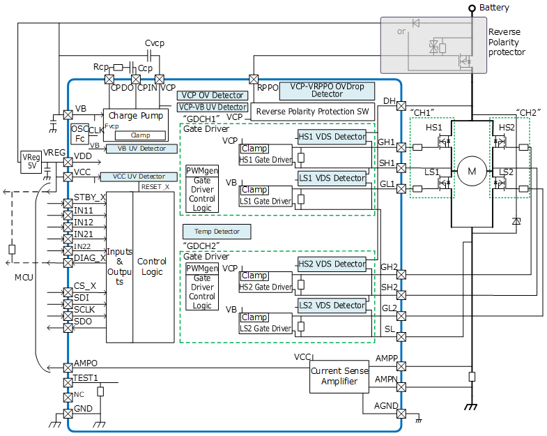
In recent years, automobiles have increasingly adopted electrification of movable components, resulting in a large number of motors installed per vehicle. In particular, the number of motors used in body-related applications has grown significantly. Consequently, the number of motor drivers has also increased, making miniaturization necessary. Additionally, the weight of wiring harnesses and other cabling has risen, so reducing wiring is required for vehicle weight reduction. To meet these demands, our company has prototyped the gate driver IC TB9104FTG, which features a compact package and adopts the serial bus SPI [Note 1], and its basic operation has been confirmed (see Figure 1).
The TB9104FTG adopts a compact VQFN32 [Note 2] package measuring 5.0mm×5.0mm (typical). A heat dissipation pad is provided on the back of the package, achieving excellent thermal performance. By using this package, the driver can be made more compact when used with an external MOSFET [Note 3].
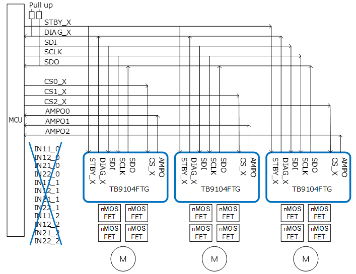
The TB9104FTG uses a serial bus SPI for communication with the microcontroller, providing numerous configuration options and status information. By connecting multiple gate drivers to the SPI, wiring can be reduced. This helps lower harness weight and simplify system design.
With the TB9104FTG, motor rotation commands can be given not only through dedicated terminals but also via SPI. In addition, it has a built-in PWM [Note 4] drive circuit. By presetting the PWM cycle and other parameters, the microcontroller only needs to issue a rotation command once, and the motor will continue to operate intermittently. This helps to reduce the load on the microcontroller and alleviate congestion on the SPI.
The TB9104FTG, as a device handling high currents, is equipped with various abnormality detection and shutdown functions. For abnormal voltage detection, it monitors VCC, VDD voltage, battery voltage, charge pump voltage, power supply voltage for reverse connection protection circuits, and drain-source voltage. In addition, it features abnormal high temperature detection and SPI error detection functions. When an abnormality is detected by these functions, the device performs a preset shutdown operation, contributing to safety.
The TB9104FTG is equipped with an amplifier that accurately amplifies the small voltage generated across the current sensing resistor, which is installed for the microcontroller to monitor the current flowing through the external MOSFET.
Key Features
- Compact Package (VQFN32)
- SPI Adoption
- Built-in PWM Drive Circuit
1. Compact Package (VQFN32)
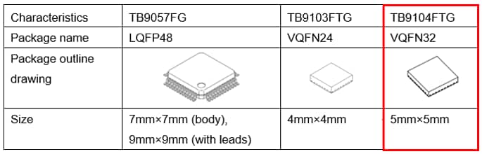
Reduces board area (Compared with our previous products). The QFN package with a heat dissipation pad on the back provides excellent thermal performance.
The TB9104FTG uses a QFN package to achieve miniaturization. It features a heat dissipation pad on the back, providing excellent thermal performance.
By combining an external MOSFET with a body that is nearly as compact as the TB9103FTG (see Figure 2), customers can reduce the board area and achieve a compact driver design.
2. SPI Adoption
By adopting an SPI, it is possible not only to finely configure operation settings and monitor status from the microcontroller, but also to issue motor rotation commands.
Settings for the TB9104FTG are made via SPI. However, there are two ways to issue motor rotation commands: using the IN11, IN12, IN21, and IN22 terminals, or by sending commands through SPI.
If you use the IN11, IN12, IN21, and IN22 terminals, you can give highly flexible commands from the microcontroller. On the other hand, by issuing commands via SPI, multiple devices can share the SPI, which helps reduce wiring. (Figure 3) In the example shown in this figure, three motors are controlled by a single microcontroller over SPI, so wiring to the IN11, IN12, IN21, and IN22 terminals is not required. Using SPI, customers can reduce wiring weight and PCB area, which contributes to lowering the overall vehicle weight.
3. Built-in PWM Drive Circuit
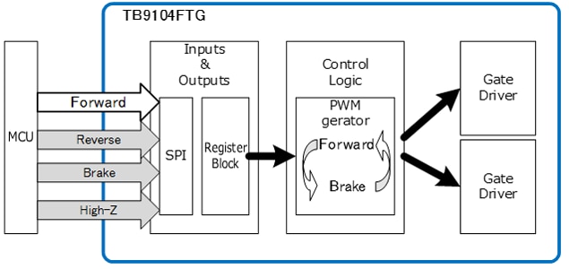
Equipped with a PWM drive circuit, the microcontroller only needs to issue a forward or reverse command once, and PWM drive with the preset cycle can be performed automatically.
The TB9104FTG can send rotation commands to the motor via SPI. However, in H-bridge operation, when using PWM drive to limit the motor’s rotational speed by alternately issuing rotation and brake commands with a delay, frequent command transmissions would be required from SPI, and rapid switching would be restricted by SPI’s speed limitations. To address this, the TB9104FTG is equipped with a built-in PWM function. Once the PWM cycle and duty ratio are set in advance, simply issuing a single rotation command to the motor will alternate between rotation and braking operations at the specified cycle and duty ratio. With this feature, even if multiple drivers are connected to the SPI, it prevents increased load on the microcontroller and avoids congestion on the SPI. (Figure 4) The PWM function can also be used when operating via the IN11 and IN12 terminals.
By reducing the load on the microcontroller, customers can consider adding more tasks or increasing the number of devices connected to the SPI.
TB9104FTG Main Specifications
Operating ranges
The power supplies (VB, VCC, VDD) are intended for use with a 12V battery system. The chip temperature range for guaranteed specifications is -40°C to 150°C, which corresponds to Grade 1 as defined by AEC-Q100.
TB9104FTG is equipped with a 2x boost charge pump, which enables it to drive the high-side N-channel power MOSFET among the external MOSFETs. The main specifications are shown below (Table 1, Table 2).
| Characteristics | Symbol | Min | Typ. | Max | Unit |
|---|---|---|---|---|---|
| Operating power supply voltage1 | VvbRNG | 5.7 | 12 | 18 | V |
| Operating power supply voltage2 | VvccRNG | 4.5 | 5.0 | 5.5 | V |
| Operating power supply voltage3 | VvddRNG | 4.5 | 5.0 | 5.5 | V |
| Operating junction temperature | TjRNG | -40 | - | 150 | °C |
Electrical Characteristics (excerpt)
Unless otherwise specified, VB=5.7 to 18V, VDD=VCC=4.5 to 5.5V(VB≧VDD) and Ta= -40 to 125°C.
All voltages are referenced to GND, and the current direction flowing into the pin is positive.
| Characteristics | Symbol | Condition | Min | Typ. | Max | Unit |
|---|---|---|---|---|---|---|
| Charge pump voltage 1 | Vvcp | VB=8 to 18V | VB+5.7 | - | VB+14.5 | V |
| Charge pump voltage 2 | VvcpL | VB=5.7 to 8V | VB+4.3 | - | VB+8 | V |
| Driving voltage between high-side gate and source when on 1 |
VgsHSsrc1 | SHx=VB, Iload=-100μA VB=8 to 18V GHx-SHx |
4 | - | 12 | V |
| Driving voltage between high-side gate and source when on 2 |
VgsHSsrc2 | SHx=VB, Iload=-100μA VB=5.7 to 8V GHx-SHx |
4 | - | 8 | V |
| Shunt voltage between high-side gate and source when off |
VgsHSsnk | SHx=VB, Iload=-100μA GHx-SHx |
- | - | 0.2 | V |
| Driving voltage between low-side gate and source when on 1 |
VgsLSsrc1 | SL=GND, Iload=-100μA VB=8 to 18V GLx-SL |
4 | - | 12 | V |
| Driving voltage between low-side gate and source when on 2 |
VgsLSsrc2 | SL=GND, Iload=-100μA VB=5.7 to 8V GLx-SL |
4 | - | 8 | V |
| Shunt voltage between low-side gate and source when off |
VgsLSsnk | SL=GND, Iload=-100μA GLx-SL |
- | - | 0.2 | V |
| Output resistance 1 | Ronh | The gate driver is on Iload=-50mA |
- | 10 | 20 | Ω |
| Output resistance 2 | Ronl | The gate driver is off Iload=50mA |
- | 3 | 6 | Ω |
Related information
Table 3. Lineup of Gate Driver IC for Automotive Brushed Motors
GD: Gate Driver, CP: Charge Pump, MCSA: Motor Current Sense Amplifier, SR: Safety Relay, Dev.: Development,
xTBV: x Times Battery Voltage
| Part number | Status | Package | GD | CP | MCSA | GD for SR | SPI | Comment |
|---|---|---|---|---|---|---|---|---|
| TB9103FTG | MP | VQFN24 | ○ (H-bridge or 2ch Half-bridge) |
○ (2TBV) |
- | - | - | Proposes replacing the mechanical relay with a semiconductor relay. |
| TB9104FTG | Dev. | VQFN32 | ○ (H-bridge or 2ch Half-bridge) |
○ (2TBV) |
○ (1ch) |
○ (1ch) |
○ |
Highly versatile product enabling detailed control via SPI. |
| TB9052FNG | MP | HTSSOP48 | ○ (H-bridge) |
○ (3TBV) |
○ (1ch) |
- | - | Adds a sequence‑generation circuit to the H‑bridge gate driver.” |
| TB9057FG | MP | LQFP48 | ○ (H-bridge) |
○ (3TBV) |
○ (1ch) |
- | - | Operation under low battery voltage, Enhanced FuSa. Built-in Phase Monitor to monitor direction of motor operation. |
[Note 1] SPI: Abbreviation of Serial Peripheral Interface.
[Note 2] QFN: Abbreviation of Quad Flat Non-leaded package.
[Note 3] MOSFET: Abbreviation of Metal Oxide Semiconductor Field Effect Transistor.
[Note 4] PWM: Abbreviation of Pulse Width Modulation.
[Note 5] FuSa: Abbreviation of Functional safety.
Queries about purchasing, sampling and IC reliability
Stock Check & Purchase
require 3 characters or more.
Through this website you are able to proceed to the website of our distributors ("Third Party Website") which is not under the control of Toshiba Corporation and its subsidiaries and affiliates (collectively "Toshiba"). The Third Party Website is made available to you as a convenience only and you agree to use the Third Party Website at your own risk. The link of the Third Party Website does not necessarily imply a recommendation or an endorsement by Toshiba of the Third Party Website. Please be aware that Toshiba is not responsible for any transaction done through the Third Party Website, and such transactions shall be subject to terms and conditions which may be provided in the Third Party Website.
* Company names, product names, and service names may be trademarks of their respective companies.