
- General Top
- SEMICONDUCTOR
- STORAGE
- COMPANY
-
My ToshibaSemicon
- Semiconductor Top
-
ApplicationsAutomotive
Body Electronics
xEV
In-Vehicle Infotainment
Advanced Driver-Assistance Systems (ADAS)
Chassis
IndustrialInfrastructure
BEMS/HEMS
Factory Automation
Commercial Equipment
Consumer/PersonalIoT Equipment
Healthcare
Wearable Device
Mobile
Computer Peripherals
-
ProductsAutomotive Devices
Discrete Semiconductor
Diodes
Transistors
Logic ICs
Analog Devices
- Automotive SmartMCD™ (Integreted SoC Conbining Microcontroller and Driver)
- Automotive Brushless Motor Driver ICs
- Automotive Brushed DC Motor Driver ICs
- Automotive Stepping Motor Driver ICs
- Automotive Driver ICs
- Automotive System Power Supplies ICs
- Automotive audio power amplifier ICs
- Automotive Network Communication
Digital Devices
Wireless Devices
※
 : Products list (parametric search)Power Semiconductors
SiC Power Devices
※
: Products list (parametric search)Isolators/Solid State RelaysPhotocouplers
Digital Isolators
Solid State Relays
Fiber Optic Transmitting Modules
※
: Products list (parametric search)MOSFETsIGBTs/IEGTsBipolar Transistors※
: Products list (parametric search)Diodes※
: Products list (parametric search)MicrocontrollersMotor Driver ICsIntelligent Power ICs※
: Products list (parametric search)Power Management ICsLinear ICs※
: Products list (parametric search)General Purpose Logic ICsLinear Image SensorsOther Product ICsOther Product ICs
※
: Products list (parametric search) -
Design & Development
-
Knowledge
- Where To Buy


- Part Number & Keyword Search
- Cross Reference Search
- Parametric Search
- Stock Check & Purchase
This webpage doesn't work with Internet Explorer. Please use the latest version of Google Chrome, Microsoft Edge, Mozilla Firefox or Safari.
require 3 characters or more. Search for multiple part numbers fromhere.
The information presented in this cross reference is based on TOSHIBA's selection criteria and should be treated as a suggestion only. Please carefully review the latest versions of all relevant information on the TOSHIBA products, including without limitation data sheets and validate all operating parameters of the TOSHIBA products to ensure that the suggested TOSHIBA products are truly compatible with your design and application.Please note that this cross reference is based on TOSHIBA's estimate of compatibility with other manufacturers' products, based on other manufacturers' published data, at the time the data was collected.TOSHIBA is not responsible for any incorrect or incomplete information. Information is subject to change at any time without notice.
require 3 characters or more.
Dual Power supply bus switch level shifter capable of voltage level conversion
Toshiba has a lineup of dual power supply level shift bus switches that can convert voltage levels.
You can select the required circuit configuration (SPST, SPDT, etc.) and the number of circuits from the product lineup.
This product group has a configuration similar to a simple switch, does not have drive capability, but is suitable for high-speed signal transmission.
Toshiba also has a product lineup of dual power bus buffers with drive capability as level shifters.
Voltage translation by Dual-supply level shift bus switches
| Product Category | Product Name |
Number of circuits |
Package | VCCA(V) | VCCB(V) | Input/Output Characteristics (translating up)(VOHU) |
Voltage translation range(V) |
Supply voltage condition |
tPLZ/tPZL(ns) @Ta=85℃ | |
|---|---|---|---|---|---|---|---|---|---|---|
| Dual supply Level shift Bus Switch |
TC7MPB9307 | SPST | 8 | TSSOP/US | 1.65 to 5.0 | 2.3 to 5.5 | 1.4@VCCA=1.65 2.05@VCCA=2.3 2.7@VCCA=3.0 |
1.4→5.5(A→B) 5.5→1.65(B→A) |
VCCA<VCCB | VCCA=3.3±0.3、VCCB=5±0.5 11/9 @RL=1kΩ,CL=30 pF VCCA=2.5±0.2, VCCB=5±0.5 15/13 @RL=1 kΩ,CL=30 pF |
| TC7MPB9326 | SPDT | 2 | ||||||||
| TC7MPB9327 | ||||||||||
| TC7QPB9306 | SPST | 4 | ||||||||
| TC7QPB9307 | ||||||||||
| TC7WPB9306 | 2 | US8 | ||||||||
| TC7WPB9307 | 2 | |||||||||
| TC7SPB9306 | 1 | UF6 | ||||||||
| TC7SPB9307 | 1 | |||||||||
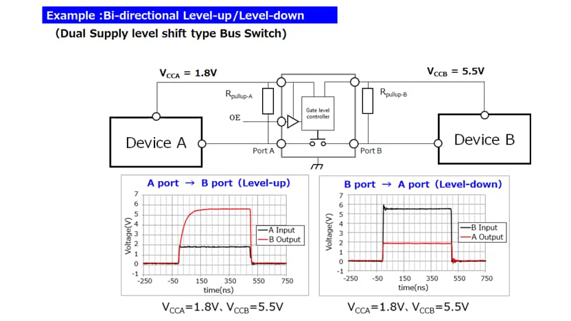
This is a 2-power supply level shift bus switch product that converts the level with an external pull-up resistor.
Since it is a bus switch type, it can be used as an interface between two power supplies without signal direction control (no DIR control).
This product can be used for I2C communication.
Single pole single throw (SPST) and single pole double throw (SPDT) products are available.
Must be used in systems with potential differences where VCCA<VCCB.
Example of level-shifting for an I2C interface
Dual supply level shift bus switch (2bit)
(TC7WPB9306FK/TC7WPB9307FK)
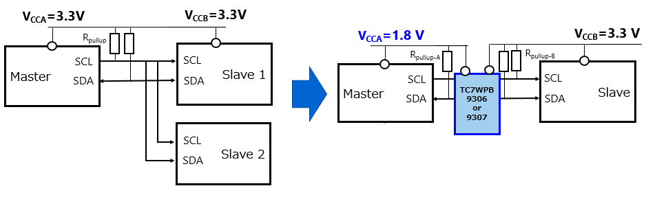
When the power supply voltage of the master device is lowered from 3.3 V to 1.8 V, the output (SCL / SDA) voltage (VOUT) from the master device falls below the input threshold (VIH) of the slave device, causing malfunction.
Also, the output (SDA) voltage of the slave device will exceed the master's power supply voltage, which can damage the master device.
In such a case, you can easily convert the signal level by placing a level shifter in between.
In the above cases, TC7WPB9306 (SDA, SCL) is an excellent choice. An external pull-up resistor (about 1 kΩ) is required to raise the output to the power supply voltage.