
- General Top
- SEMICONDUCTOR
- STORAGE
- COMPANY
-
My ToshibaSemicon
- Semiconductor Top
-
ApplicationsAutomotive
Body Electronics
xEV
In-Vehicle Infotainment
Advanced Driver-Assistance Systems (ADAS)
Chassis
IndustrialInfrastructure
BEMS/HEMS
Factory Automation
Commercial Equipment
Consumer/PersonalIoT Equipment
Healthcare
Wearable Device
Mobile
Computer Peripherals
-
ProductsAutomotive Devices
Discrete Semiconductor
Diodes
Transistors
Logic ICs
Analog Devices
Digital Devices
Wireless Devices
※
 : Products list (parametric search)Power Semiconductors
SiC Power Devices
※
: Products list (parametric search)Isolators/Solid State RelaysPhotocouplers
Digital Isolators
Solid State Relays
Fiber Optic Transmitting Modules
※
: Products list (parametric search)MOSFETsIGBTs/IEGTsBipolar Transistors※
: Products list (parametric search)Diodes※
: Products list (parametric search)MicrocontrollersMotor Driver ICsIntelligent Power ICs※
: Products list (parametric search)Power Management ICsLinear ICs※
: Products list (parametric search)General Purpose Logic ICsLinear Image SensorsOther Product ICsOther Product ICs
※
: Products list (parametric search) -
Design & Development
-
Knowledge
- Where To Buy


- Part Number & Keyword Search
- Cross Reference Search
- Parametric Search
- Stock Check & Purchase
This webpage doesn't work with Internet Explorer. Please use the latest version of Google Chrome, Microsoft Edge, Mozilla Firefox or Safari.
require 3 characters or more. Search for multiple part numbers fromhere.
The information presented in this cross reference is based on TOSHIBA's selection criteria and should be treated as a suggestion only. Please carefully review the latest versions of all relevant information on the TOSHIBA products, including without limitation data sheets and validate all operating parameters of the TOSHIBA products to ensure that the suggested TOSHIBA products are truly compatible with your design and application.Please note that this cross reference is based on TOSHIBA's estimate of compatibility with other manufacturers' products, based on other manufacturers' published data, at the time the data was collected.TOSHIBA is not responsible for any incorrect or incomplete information. Information is subject to change at any time without notice.
require 3 characters or more.
What is the difference between MOSFETs and IGBTs?
The main differences between IGBTs and MOSFETs are their on-resistance and switching speed. MOSFETs have a fast-switching speed, but in order to increase the breakdown voltage, the concentration of the n- drift layer must be reduced, resulting in a high series resistance (n- drift resistance). Because IGBTs are bipolar devices, they use the conductivity modulation effect to reduce the n- drift resistance when on, but this effect generates a tail current when off, slowing down the switching speed. MOSFETs are unipolar devices that use only electrons as carriers, while IGBTs are bipolar devices that use both electrons and holes.

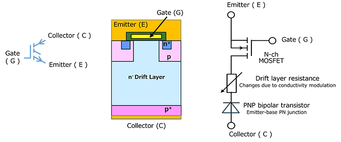
1. Structure
IGBT (Insulated Gate Bipolar Transistor) is also a voltage-controlled element with an insulated gate, similar to MOSFET (Metal Oxide Semiconductor Field Effect Transistor). IGBT has a structure in which a p+ layer is added to the n+ layer on the back side (drain side) of the MOSFET chip, and this layer functions as the collector. Fig. 1 and 2 show the structure and equivalent circuit of IGBT and MOSFET. An important feature of IGBT is conductivity modulation.
2. Operation
Compared to bipolar junction transistors (BJTs), MOSFETs and IGBTs have the advantage of having high input impedance and fast switching speeds due to the insulated gate.
In MOSFETs and IGBTs, when the voltage between the gate and source or between the gate and emitter is equal to or greater than the threshold voltage, conduction occurs between the drain and source or between the collector and emitter, and the MOSFET turns on.
The on-resistance of a MOSFET is greatly affected by the resistance of the n- drift layer. In order to increase the breakdown voltage of a MOSFET, it is necessary to reduce the concentration of the n-drift layer and make it thicker, which results in an issue of higher on-resistance. On the other hand, IGBTs reduce the on-resistance by reducing the resistance of the n- drift layer through conductivity modulation, as will be described below.
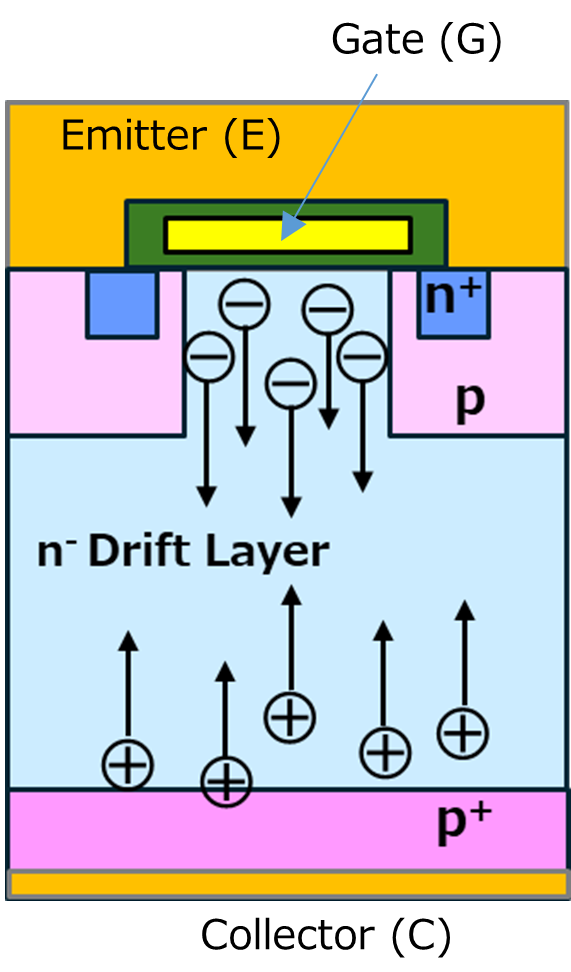
Fig. 3 shows the behavior of carriers (holes and electrons) in the conductivity modulation of an IGBT. When no conductivity modulation occurs in an IGBT, the n- layer contains a small amount of electrons, but when in the on state, holes are injected from the p+ collector layer into the n- layer. If this continues, the density of holes in the n- layer will exceed the equilibrium value. To maintain charge neutrality, electrons are injected from the n+ layer through the channel into the n- drift layer, maintaining electrical neutrality. This increases the density of both majority carriers (holes) and minority carriers (electrons) in the n- drift layer, significantly improving conductivity. Therefore, the on-resistance of an IGBT is lower than that of a MOSFET, and the on-voltage is also lower.
When the gate-source or gate-emitter of a MOSFET or IGBT is short-circuited or reverse-biased, the gate charge is discharged, the channel disappears, and the MOSFET or IGBT turns off. However, in an IGBT, excess carriers (electrons and holes) accumulate in the n-region due to conductivity modulation when the MOSFET is on. In a MOSFET, the drain current is cut off more quickly than in an IGBT, but when an IGBT is turned off, it takes time for the collector current to continue to flow as it decreases until the excess carriers dissipate. This gradually decreasing current is called the tail current.
3. Comparison of MOSFET and IGBT characteristics
There are three typical types of transistors: bipolar transistors (BJT), MOSFET, and IGBT. Table 1 shows the general performance and characteristics of each transistor. Due to the characteristics of drive power and switching speed of drive circuits, BJTs are rarely used for switching applications in the power electronics field, and MOSFETs and IGBTs are mainly used, taking advantage of their respective features.
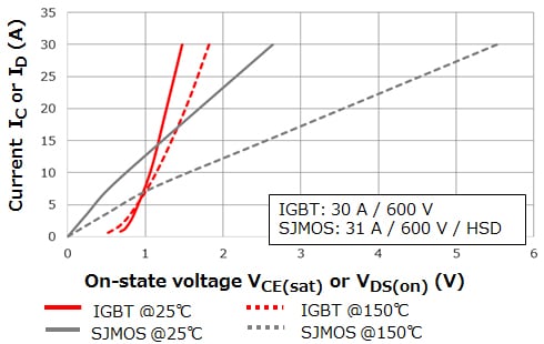
Fig. 4 shows the on-voltage characteristics of a 30A class IGBT and MOSFET (SJMOS: Super-junction MOSFET). In the low current region, MOSFETs exhibit lower on-voltage characteristics than IGBTs, but in the high current region, IGBTs are superior, and this tendency is particularly noticeable under high temperature conditions. Also, compared to MOSFETs, which are unipolar devices, IGBTs have larger switching losses, so they are often used at switching frequencies lower than around 20 kHz.
| BJT | MOSFET | IGBT | |
|---|---|---|---|
| Drive type | Current drive |
Voltage drive |
Voltage drive |
| Power for driving | High | Low | High |
| On state voltage | Moderate | Tends to increase in |
Low |
| Switching speed | Low |
High |
Moderate |
| Temperature stability | Poor | Good | Good |
| Difficulty of achieving high breakdown voltage |
Moderate | High | Easy with conductivity modulation |
Related Links
The following documents also contain related information.
Parametric Search
IGBTs/IEGTs
FAQs
* Company names, product names, and service names used in this FAQ may be of their respective companies.