
- General Top
- SEMICONDUCTOR
- STORAGE
- COMPANY
-
My ToshibaSemicon
- Semiconductor Top
-
ApplicationsAutomotive
Body Electronics
xEV
In-Vehicle Infotainment
Advanced Driver-Assistance Systems (ADAS)
Chassis
IndustrialInfrastructure
BEMS/HEMS
Factory Automation
Commercial Equipment
Consumer/PersonalIoT Equipment
Healthcare
Wearable Device
Mobile
Computer Peripherals
-
ProductsAutomotive Devices
Discrete Semiconductor
Diodes
Transistors
Logic ICs
Analog Devices
- Automotive SmartMCD™ (Integreted SoC Conbining Microcontroller and Driver)
- Automotive Brushless Motor Driver ICs
- Automotive Brushed DC Motor Driver ICs
- Automotive Stepping Motor Driver ICs
- Automotive Driver ICs
- Automotive System Power Supplies ICs
- Automotive audio power amplifier ICs
- Automotive Network Communication
Digital Devices
Wireless Devices
※
 : Products list (parametric search)Power Semiconductors
SiC Power Devices
※
: Products list (parametric search)Isolators/Solid State RelaysPhotocouplers
Digital Isolators
Solid State Relays
Fiber Optic Transmitting Modules
※
: Products list (parametric search)MOSFETsIGBTs/IEGTsBipolar Transistors※
: Products list (parametric search)Diodes※
: Products list (parametric search)MicrocontrollersMotor Driver ICsIntelligent Power ICs※
: Products list (parametric search)Power Management ICsLinear ICs※
: Products list (parametric search)General Purpose Logic ICsLinear Image SensorsOther Product ICsOther Product ICs
※
: Products list (parametric search) -
Design & Development
-
Knowledge
- Where To Buy


- Part Number & Keyword Search
- Cross Reference Search
- Parametric Search
- Stock Check & Purchase
This webpage doesn't work with Internet Explorer. Please use the latest version of Google Chrome, Microsoft Edge, Mozilla Firefox or Safari.
require 3 characters or more. Search for multiple part numbers fromhere.
The information presented in this cross reference is based on TOSHIBA's selection criteria and should be treated as a suggestion only. Please carefully review the latest versions of all relevant information on the TOSHIBA products, including without limitation data sheets and validate all operating parameters of the TOSHIBA products to ensure that the suggested TOSHIBA products are truly compatible with your design and application.Please note that this cross reference is based on TOSHIBA's estimate of compatibility with other manufacturers' products, based on other manufacturers' published data, at the time the data was collected.TOSHIBA is not responsible for any incorrect or incomplete information. Information is subject to change at any time without notice.
require 3 characters or more.
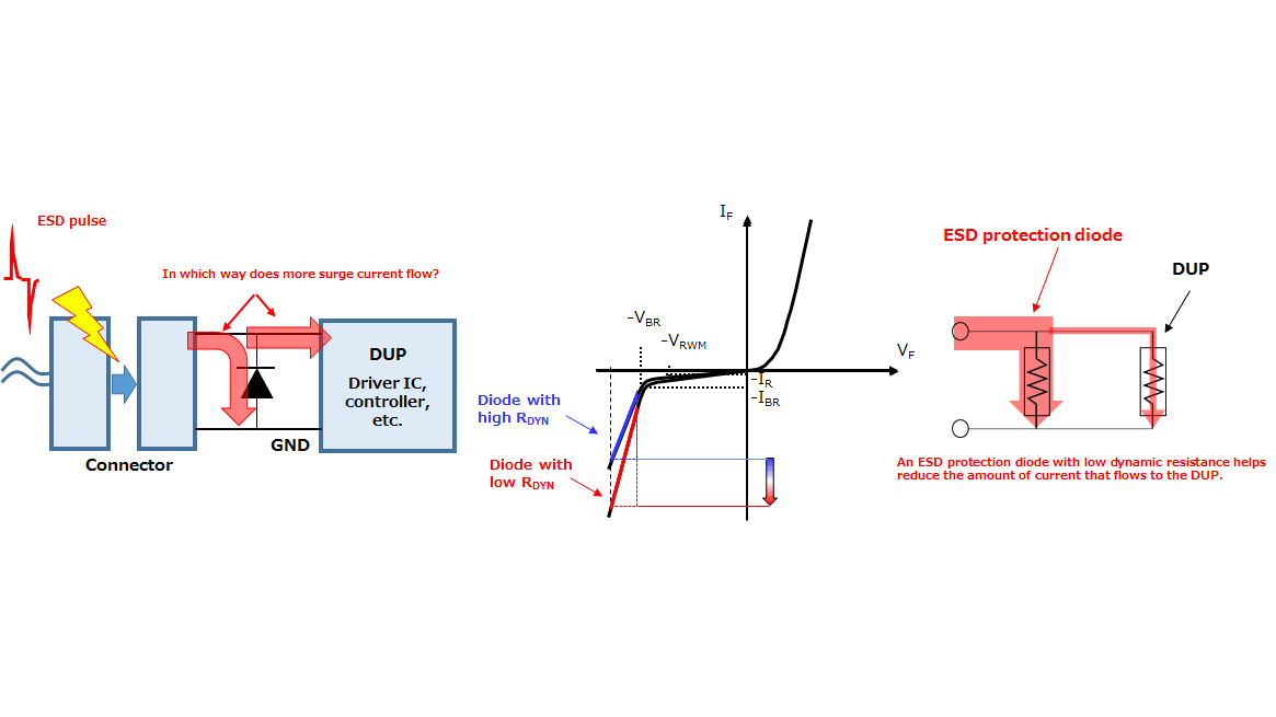
3-3-2. Key characteristics for protection against ESD events(2)
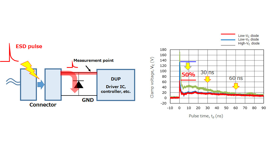
3-3-2. Low clamp voltage (VC) and first peak voltage
Figure 3.10 shows the response waveforms of ESD protection diodes with high and low clamp voltages (VC) when an ESD waveform stipulated in IEC 61000-4-2 was applied to them. These waveforms were taken at the input of a device under protection (DUP). The ESD protection diode with a lower VC exhibits lower clamp voltage at 30 ns and 60 ns than the one with a higher VC. The smaller the area under the curve of the ESD waveform, the less damage the DUP suffers. Therefore, ESD protection diodes with low VC provide better protection against ESD pulses. In addition, some ESD protection diodes do not respond immediately after the ESD entry. Therefore, if the first peak of the ESD pulse is higher than the VC of the ESD protection diode, it might be applied to the DUP, leading to its malfunction or destruction. ESD protection diodes are designed to provide faster response than other types of protection devices. In addition, Toshiba is working on the optimization of the chip process and the internal device structure in order to further reduce the first peak voltage and therefore provide more rugged protection against the peak ESD voltage during the initial period.
3. Key electrical characteristics of TVS diodes (ESD protection diodes)


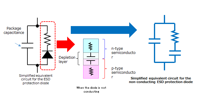

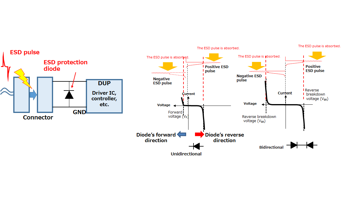
- 1. What is a TVS diode (ESD protection diode)?
- 2. Basic operations of TVS diodes (ESD protection diodes)
- 4. Selection guidelines for TVS diodes (ESD protection diodes)
- 5. Layout considerations for TVS diodes (ESD protection diodes)
- 6. Absolute maximum ratings of TVS diodes (ESD protection diodes)
- 7. Electrical characteristics of TVS diodes (ESD protection diodes)
Related information
- Product Web Page
TVS Diodes (ESD protection diodes) - Applidcation Notes
Diode - FAQ
TVS diodes (ESD protection diodes) - Parametric searches for all Toshiba TVS diode (ESD protection diodes) produ cts are available here:
Parametric search - Stock Check & Purchase Toshiba TVS diode (ESD protection diodes) here
Stock Check & Purchase