How do I choose an ESD protection diode?
When selecting ESD protection diodes for general interface applications, the requirements for both normal operation and ESD protection should be considered. The following summarizes how to select ESD protection diodes. The selection process is detailed later.
- When a system is operating normally without ESD entry
ESD protection diodes do nothing during normal operation. They should not affect the protected signal lines.- Select ESD protection diodes with working peak reverse voltage (VRWM) higher than the maximum voltage of the protected lines.
- Select unidirectional ESD protection diodes for positive unipolar signals and bidirectional ESD protection diodes for bipolar signals.
- Select ESD protection diodes with total capacitance (CT) suitable for the frequency of the protected signal lines.
- When excessive voltage or current due to ESD enters a board.
It is crucial to reduce the ESD energy to a level that does not destroy the device under protection (DUP).- Select ESD protection diodes with low clamp voltage (VC).
- Select ESD protection diodes with low dynamic resistance (RDYN).
Two different materials that are far away from each other in the triboelectric series tend to acquire a positive or negative charge when they come into close contact. When they are rubbed together, the friction causes one to lose electrons and be positively charged while the other gains electrons and becomes negatively charged. (See the FAQ entry “What is electrostatic discharge (ESD)?”
What is electrostatic discharge (ESD)?
When a charged object touches a connector of an electronic device, the charge is released instantaneously as a current pulse. Called an electrostatic discharge (ESD), this phenomenon is akin to the discharging of a capacitor.
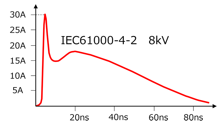
Figure 1 shows the IEC 61000-4-2 ESD waveform that is widely known as an ESD simulation waveform. As you see, the ESD current rises sharply to 30 A in roughly 1 ns.
The ESD energy that enters a board depends on the output impedance (i.e., the specific resistance of a material) on the transmitter side and the input impedance on the receiver side. However, an ESD surge has much higher voltage and current than a signal during normal operation. Therefore, an ESD strike could degrade or destroy an internal device of a system.
There are several catastrophic failure modes. Here are three examples of semiconductor destruction:
- Failure caused by high voltage: A short-circuit due to dielectric punch-through caused by a voltage higher than the electric breakdown strength of the gate oxide
- Failure caused by high current: An open-circuit caused by an excessive current flowing into resistors and wires in a semiconductor device
- Failure caused by high voltage and current: A short-circuit caused by the destruction of a pn junction due to ESD energy
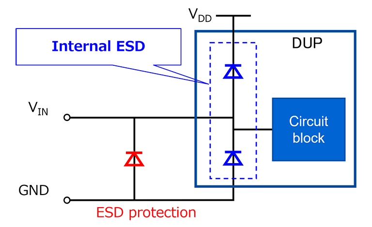
Generally, ESD-sensitive ICs incorporate ESD protection circuitry. Its purpose is to protect ICs from ESD in electronics manufacturing facilities. Therefore, the internal ESD protection circuitry is intended for device-level protection in an ESD-controlled environment. The system-level ESD that you experience in daily life has higher energy than it can handle. (For a description of device-level and system-level ESD, see the FAQ entry “Electrostatic discharge (ESD) testing.”
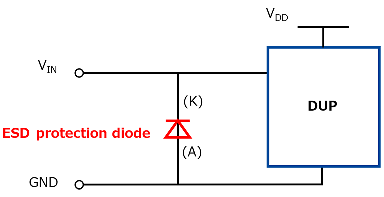
For protection against system-level ESD, an external ESD protection diode is connected between a signal line and GND as shown in Figure 2. Signal lines that could be an ESD entry point require ESD protection diodes, including externally exposed I/O ports for connectors and touch sensors as well as the VIN line connected to antennas.
Adding ESD protection diodes is not enough. It is important to select the right ESD protection diodes according to the signal lines to be protected and circuit conditions. In addition, you need to optimize the placement of ESD protection diodes in order to obtain the best protection performance. For the placement of ESD protection diodes, see the FAQ entry “Board design considerations for TVS diodes (ESD protection diodes)”.
Board design considerations for TVS diodes (ESD protection diodes)
The following discusses the electrical characteristics required for normal operation and ESD protection summarized at the beginning of this FAQ.
- When a system is operating normally without ESD
- When excessive voltage or current due to ESD enters a board
- When a system is operating normally without ESD
It is important to ensure that ESD protection diodes do not affect the signal integrity of the signal and control lines to which they are connected. Ideally, ESD protection diodes should be open in the off state (with infinite impedance), but they are not in reality. ESD protection diodes are a type of Zener diodes consisting of a pn junction. Therefore, a small leakage current (reverse current, IR) flows even when they are off. IR increases as reverse bias approaches the reverse breakdown voltage, VBR (Zener voltage). Therefore, IR can be a problem, depending on the required system specifications.
IR is the current that flows when the prescribed reverse voltage is applied across a diode as shown in Figure 3. IR differs from diode to diode and ranges from 0.05 μA to 2.5 μA. In the case of ESD protection diodes, IR is specified at working peak reverse voltage (VRWM).
Suppose that a 47-kΩ pull-up resistor is connected to the output of a DUP. Then, in the case of an ESD protection diode with an IR of 2.5 μA, the pull-up resistor causes a 118-mV decrease in signal voltage Since application of a voltage higher than VRWM to the DUP causes an exponential increase in current, the maximum voltage of the signal line to be protected must be lower than the VRWM of the ESD protection diode.

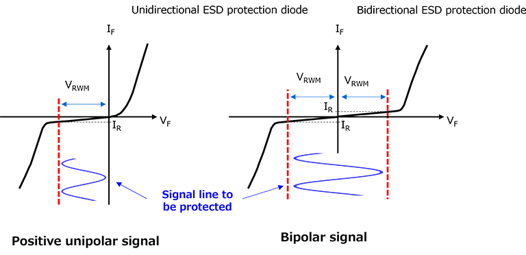
In the case of bipolar signals, select bidirectional ESD protection diodes. In this case, the minimum and maximum voltages of the signal line to be protected must be lower than VRWM. (For bidirectional ESD protection diodes, see the following FAQ entry.)
FAQ: Is it necessary to use bidirectional TVS diodes (ESD protection diodes) to protect against both positive and negative ESD events?
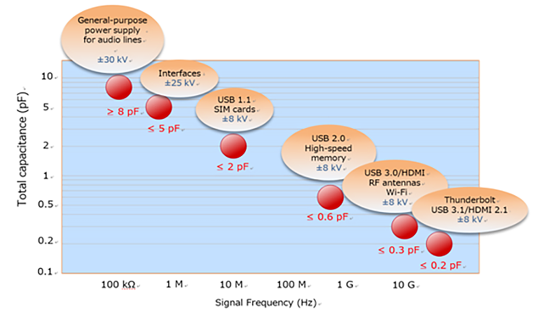
When a diode is off, a depletion region is formed across the pn junction. The depletion region can be viewed as a capacitor externally. Therefore, the total capacitance (CT) of an ESD protection diode is defined as the sum of the depletion region capacitance and parasitic capacitance. It is necessary to select ESD protection diodes with low total capacitance to protect high-frequency signal lines. Use Figure 5 as a guide to select ESD protection diodes with appropriate total capacitance.
See the following e-learning course for the depletion region capacitance.
e-learning: Variable-capacitance Diodes (Varicap Diodes)
2. When excessive voltage or current due to ESD enters a board
ESD protection diodes should turn on upon ESD entry to clamp the voltage surge to reduce the voltage applied to the DUP. It is therefore necessary to select ESD protection diodes with low clamp voltage (VC) while considering the constraint for VRWM during normal operation.
Here, let us see the operating conditions of the DUP.
As mentioned above, ESD-sensitive devices incorporate ESD protection circuitry. Figure 6 shows an example of an ESD protection circuit, which consists of two pn junction diodes.
Look at Figure 7. The internal ESD protection diodes turn on to clamp the input voltage when the signal applied to VIN or the ESD voltage level exceeds the sum of the supply voltage (VDD) and the diode’s forward voltage (VF) or drops below GND – VF. The internal ESD protection circuit is intended for device-level ESD protection. Application of an ESD voltage higher than its clamp voltage could lead to the degradation or destruction of the DUP. The red dot in Figure 7 indicates the threshold above which the DUP is destroyed by ESD.
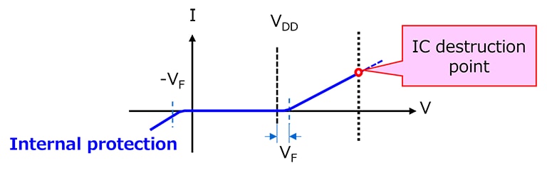
Figure 8 shows the I-V curve of an external ESD protection diode. (Note: In this figure, the positive direction represents reverse voltage (VR) to match the direction of the internal protection diodes of an IC.) The ESD protection diode enters reverse conduction mode at reverse breakdown voltage (VBR) and forward conduction mode at forward voltage (VF).
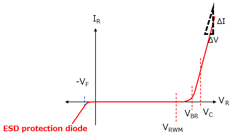
Unlike the internal protection circuitry of an IC, the ESD protection diode provides low dynamic resistance (RDYN), causing the diode current to rise sharply in both the forward and reverse directions. Low dynamic resistance means a small change in clamp voltage. Therefore, even in the event of an ESD strike with large energy, the voltage applied to the DUP does not vary greatly. (This means the protection performance of the ESD protection diode does not vary significantly.)
Low dynamic resistance is due to Zener breakdown (or avalanche breakdown) in reverse bias as well as a wide junction area and a fabrication process specifically designed to achieve a sharp rise in the diode current.
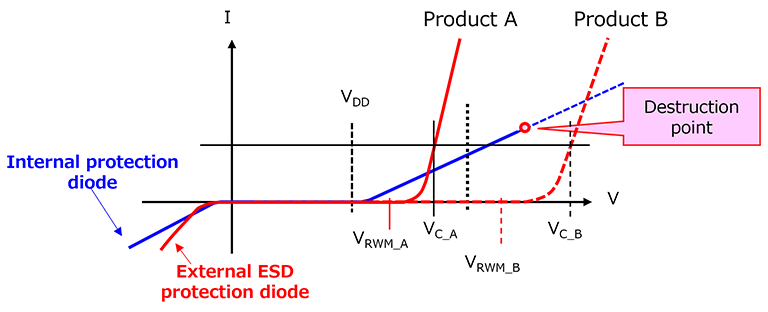
Let us consider the clamp voltage of ESD protection diodes.
Suppose that the signal line to be protected swings between 0 V and VDD. Therefore, the VRWM of ESD protection diodes must be greater than VDD. Figure 9 shows two ESD protection diodes with different clamp voltages (VC) that satisfy this requirement (Product A and Product B). Suppose that the clamp voltage of Product A (VC_A) is lower than that of Product B (VC_B). Upon ESD entry, both the external ESD protection diode and the internal ESD protection circuit of the DUP turn on. The signal line voltage at which they turn on mainly depends on the external ESD protection diode.
As you see, Product B turns on at voltage and current higher than the destruction point. So, Product B cannot be used to protect the DUP.
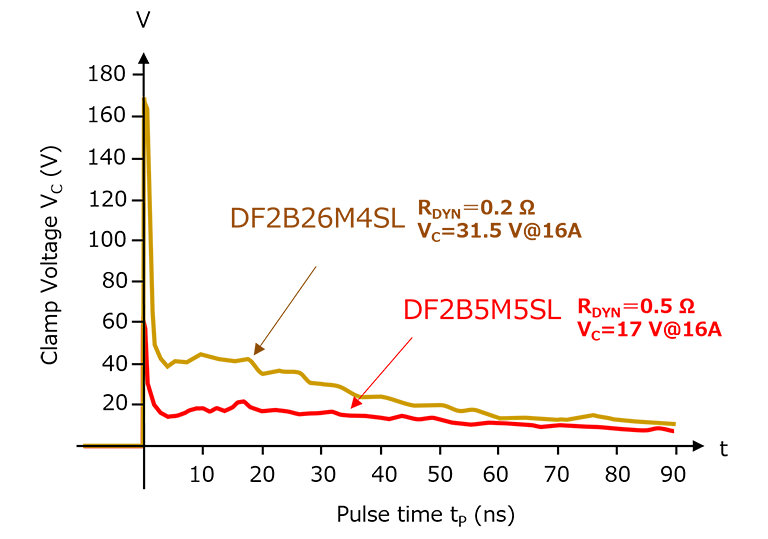
Figure 10 shows the ESD clamping waveforms of two products with different clamp voltages.
ESD protection diodes with low clamp voltage help enhance the system safety.
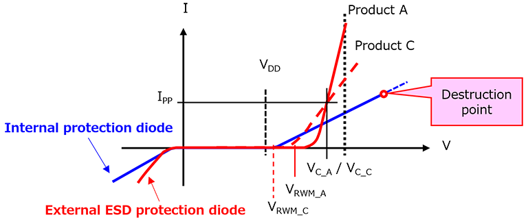
Next, let us consider two ESD protection diodes with equal clamp voltage and different dynamic resistances, RDYN (Product A and Product C).
Here, RDYN_A < RDYN_C.
Figure 11 indicates that, in the high-current region (i.e., at a voltage higher than the clamp voltage, VC), more current flows to an external ESD protection diode than to the internal protection diodes of the DUP. When compared at the same current, the voltage across the internal protection diodes is lower than the voltage across an external ESD protection diode. This means that the ESD protection diode helps reduce the stress on the DUP due to an ESD strike. Therefore, if two ESD protection diodes provide the same clamp voltage, it is advisable to select the one with lower dynamic resistance.
Related Links
For TVS diode (ESD protection diode) products, please refer to the following links.