- General Top
- SEMICONDUCTOR
- STORAGE
- COMPANY
-
My ToshibaSemicon
- Semiconductor Top
-
ApplicationsAutomotive
Body Electronics
xEV
In-Vehicle Infotainment
Advanced Driver-Assistance Systems (ADAS)
Chassis
IndustrialInfrastructure
BEMS/HEMS
Factory Automation
Commercial Equipment
Consumer/PersonalIoT Equipment
Healthcare
Wearable Device
Mobile
Computer Peripherals
-
ProductsAutomotive Devices
Discrete Semiconductor
Diodes
Transistors
Logic ICs
Analog Devices
- Automotive SmartMCD™ (Integreted SoC Conbining Microcontroller and Driver)
- Automotive Brushless Motor Driver ICs
- Automotive Brushed DC Motor Driver ICs
- Automotive Stepping Motor Driver ICs
- Automotive Driver ICs
- Automotive System Power Supplies ICs
- Automotive audio power amplifier ICs
- Automotive Network Communication
Digital Devices
Wireless Devices
※
 : Products list (parametric search)Power Semiconductors
SiC Power Devices
※
: Products list (parametric search)Isolators/Solid State RelaysPhotocouplers
Digital Isolators
Solid State Relays
Fiber Optic Transmitting Modules
※
: Products list (parametric search)MOSFETsIGBTs/IEGTsBipolar Transistors※
: Products list (parametric search)Diodes※
: Products list (parametric search)MicrocontrollersMotor Driver ICsIntelligent Power ICs※
: Products list (parametric search)Power Management ICsLinear ICs※
: Products list (parametric search)General Purpose Logic ICsLinear Image SensorsOther Product ICsOther Product ICs
※
: Products list (parametric search) -
Design & Development
-
Knowledge
- Where To Buy


- Part Number & Keyword Search
- Cross Reference Search
- Parametric Search
- Stock Check & Purchase
This webpage doesn't work with Internet Explorer. Please use the latest version of Google Chrome, Microsoft Edge, Mozilla Firefox or Safari.
require 3 characters or more. Search for multiple part numbers fromhere.
The information presented in this cross reference is based on TOSHIBA's selection criteria and should be treated as a suggestion only. Please carefully review the latest versions of all relevant information on the TOSHIBA products, including without limitation data sheets and validate all operating parameters of the TOSHIBA products to ensure that the suggested TOSHIBA products are truly compatible with your design and application.Please note that this cross reference is based on TOSHIBA's estimate of compatibility with other manufacturers' products, based on other manufacturers' published data, at the time the data was collected.TOSHIBA is not responsible for any incorrect or incomplete information. Information is subject to change at any time without notice.
require 3 characters or more.
What is Electrostatic discharge (ESD) testing?
ESD (Electrostatic Discharge) testing is a method used to evaluate how much tolerance semiconductor devices and electronic equipment have when they are exposed to electrostatic discharge (ESD). ESD testing is broadly classified into device-level testing and system-level testing, based on differences in evaluation targets and test objectives.
For an explanation of the ESD phenomenon itself, please refer to the following FAQ:
> What is electrostatic discharge (ESD)?
Device-Level Testing
Device-level testing is an ESD test performed on individual semiconductor devices, such as ICs and discrete components.
This testing is conducted to confirm that a device does not suffer degradation or damage when exposed to electrostatic discharge that is assumed to occur during manufacturing, assembly, and handling processes.
The main purpose of device-level ESD testing is to evaluate whether the device under test (DUT) is degraded or damaged by ESD stress assumed during semiconductor manufacturing and assembly processes.
For this reason, test results are generally expressed as Pass / Fail (Go / No-Go) based on the presence or absence of damage.
Representative device-level ESD test models include the following:
- Human Body Model (HBM)
This test simulates a situation in which a person charged with static electricity discharges upon touching an IC or a component. - Machine Model (MM)
This test simulates a situation in which semiconductor manufacturing equipment or metal fixtures become charged and discharge to a device through a low-impedance path. - Charged Device Model (CDM)
This test simulates a situation in which the device itself becomes charged and then discharges when it comes into contact with a grounded metal object.
HBM and MM are tests in which electric charge stored in a capacitor is discharged into the device under test.
In contrast, CDM is a test in which the device itself is charged and then discharges its stored charge.
These tests are generally performed on the terminals of the device.
Protection against device-level ESD is provided by ESD protection circuits integrated into each device.
System-Level Testing
System-level testing is an ESD test performed on electronic equipment or systems under conditions close to actual usage environments.
This testing simulates ESD events that may occur in daily use environments, such as connecting cables to USB ports or human contact with connectors and touch panels.
A representative standard for system-level testing is IEC 61000-4-2.
The primary test targets are externally exposed I/O terminals, such as connectors, touch sensors, and antennas.
In system-level ESD testing, ESD waveforms with much larger peak currents are applied compared with device-level testing.
As a result, ESD protection circuits integrated into devices alone may not provide sufficient protection, and countermeasures that combine external ESD protection diodes (TVS diodes) are commonly implemented.
For details on IEC 61000-4-2 and ESD protection diodes, please refer to the following FAQ:
> What is IEC61000-4-5?
> What is an ESD protection diode?
Evaluation Concepts in System-Level Testing
In system-level ESD testing, the impact on functional operation is an important evaluation target, in addition to whether the equipment is physically damaged.
Evaluation is performed based on the following aspects:
- Whether normal operation is maintained during and after testing
- Whether temporary malfunctions or functional degradation occur
- Whether automatic recovery occurs after a malfunction
- Whether manual recovery, such as a reset operation, is required
- Whether permanent failure or loss of functionality occurs
System-level ESD testing uses a concept of stepwise evaluation of equipment immunity.
Therefore, evaluation is not limited to simple Go / No-Go judgments based solely on physical damage.
ESD Test Waveforms and TLP Measurement
Figure 1 shows examples of ESD test waveforms for device-level testing (HBM) and system-level testing (IEC 61000-4-2). Because test conditions such as impedance differ, these waveforms cannot be directly compared. System-level testing involves waveforms with very large peak currents.
This is because system-level testing specifies more severe conditions that assume difficult-to-control ESD events occurring in general usage environments.

Device-level testing and system-level testing differ significantly in ESD waveforms and current conditions. At the same time, both types of standardized testing aim to evaluate whether devices or equipment can withstand ESD stress under specified conditions.
Positioning of TLP Measurement
In ESD protection design, it is important to understand not only pass/fail results of standardized tests, but also the voltage and current characteristics exhibited by devices and ESD protection components when ESD stress is applied. Based on these design requirements, it has become increasingly common to present electrical characteristics obtained by applying short pulses similar to ESD to IC I/O terminals and ESD protection devices in datasheets.
One such characteristic evaluation method is TLP (Transmission Line Pulse) measurement.
TLP measurement is an evaluation method used to understand the electrical tolerance and clamping characteristics of devices under ESD stress, and it is utilized in ESD protection design, such as the selection of protection components. However, TLP measurement does not replace system-level ESD testing. For some products and series of our ESD protection diodes, TLP waveforms such as those shown in Figure 2 are provided as reference information in datasheets.
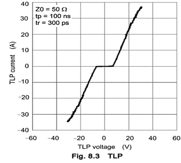
For more details on TLP testing, please refer to the following FAQ:
> What is a TLP test?
Related Links
For TVS diode (ESD protection diode) products, please refer to the following links.