- General Top
- SEMICONDUCTOR
- STORAGE
- COMPANY
-
My ToshibaSemicon
- Semiconductor Top
-
ApplicationsAutomotive
Body Electronics
xEV
In-Vehicle Infotainment
Advanced Driver-Assistance Systems (ADAS)
Chassis
IndustrialInfrastructure
BEMS/HEMS
Factory Automation
Commercial Equipment
Consumer/PersonalIoT Equipment
Healthcare
Wearable Device
Mobile
Computer Peripherals
-
ProductsAutomotive Devices
Discrete Semiconductor
Diodes
Transistors
Logic ICs
Analog Devices
- Automotive SmartMCD™ (Integreted SoC Conbining Microcontroller and Driver)
- Automotive Brushless Motor Driver ICs
- Automotive Brushed DC Motor Driver ICs
- Automotive Stepping Motor Driver ICs
- Automotive Driver ICs
- Automotive System Power Supplies ICs
- Automotive audio power amplifier ICs
- Automotive Network Communication
Digital Devices
Wireless Devices
※
 : Products list (parametric search)Power Semiconductors
SiC Power Devices
※
: Products list (parametric search)Isolators/Solid State RelaysPhotocouplers
Digital Isolators
Solid State Relays
Fiber Optic Transmitting Modules
※
: Products list (parametric search)MOSFETsIGBTs/IEGTsBipolar Transistors※
: Products list (parametric search)Diodes※
: Products list (parametric search)MicrocontrollersMotor Driver ICsIntelligent Power ICs※
: Products list (parametric search)Power Management ICsLinear ICs※
: Products list (parametric search)General Purpose Logic ICsLinear Image SensorsOther Product ICsOther Product ICs
※
: Products list (parametric search) -
Design & Development
-
Knowledge
- Where To Buy


- Part Number & Keyword Search
- Cross Reference Search
- Parametric Search
- Stock Check & Purchase
This webpage doesn't work with Internet Explorer. Please use the latest version of Google Chrome, Microsoft Edge, Mozilla Firefox or Safari.
require 3 characters or more. Search for multiple part numbers fromhere.
The information presented in this cross reference is based on TOSHIBA's selection criteria and should be treated as a suggestion only. Please carefully review the latest versions of all relevant information on the TOSHIBA products, including without limitation data sheets and validate all operating parameters of the TOSHIBA products to ensure that the suggested TOSHIBA products are truly compatible with your design and application.Please note that this cross reference is based on TOSHIBA's estimate of compatibility with other manufacturers' products, based on other manufacturers' published data, at the time the data was collected.TOSHIBA is not responsible for any incorrect or incomplete information. Information is subject to change at any time without notice.
require 3 characters or more.
What is the difference between CMOS logic IC 04 (inverter) and U04 (unbuffered inverter)?
CMOS logic ICs have an inverter as a standard function, and there are "04" and "U04". "04" is used for general logic processing (digital signal processing), and "U04" is mainly used for oscillators such as crystal oscillation circuits and RC oscillation circuits.
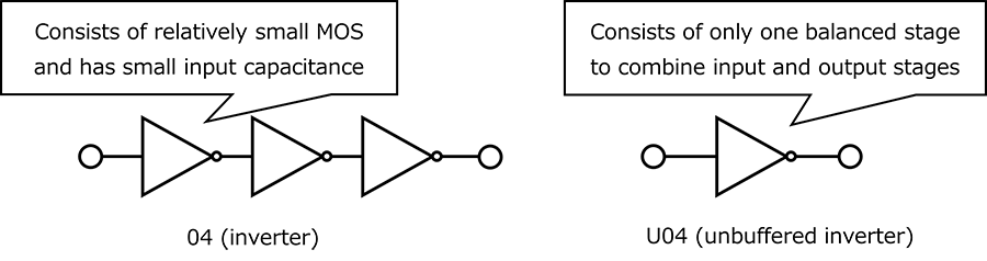
- 04: It has a 3-stage inverter configuration, the first stage is optimized for the input, and the final stage has a function as a buffer.
- U04 : Consists of a single inverter stage that has both an input stage and an output stage (buffer stage).
“04” and “U04” are configured as shown in Fig. 1. "04" has optimized MOS size for the required performance of input block and output. As a result, in the same group (family), the input capacitance of "04" is smaller than that of “U04”. "04" has a high gain due to its 3-stage configuration. In addition, the High-level / Low-level input voltage range (VIL, VIH) for judging "H" and "L" is wider than that of "U04" (Table 1), and the noise margin is high. However, the propagation delay time will be slightly longer.
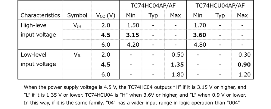

Fig. 2 shows a conceptual diagram of an oscillator circuit that uses an inverter.
Disturbances such as noise at power-on become the seeds of oscillation and enter the input Vin. These seeds are so small that it is amplified in the linear region of the inverter, filtered in the feedback circuit and summed to the input. The conditions for oscillation are that the phase of the feedback signal is in phase with the input signal, and that the gain of the inverter is large (the magnitude of the "input" + "feedback signal" is greater than the original input signal).
“04” has a small input capacitance, so it has a wide band and high gain. It can oscillate up to a higher frequency than “U04”. Considering only this point, it seems that "04" is more suitable for oscillation than "U04". However, the linear region used for oscillation is outside the region shown in Table 1 (for example, at 4.5 V, "04" is 1.35 V to 3.15 V and "U04" is 0.90 V to 3.6 V), so "U04" is wider. The oscillation signal must circulate within this range for stable oscillation. Considering more stable oscillation at the desired frequency, it is recommended to use "U04" in the oscillation circuit.
Related Links
The following documents also contain related information.
Please refer to the following e-Learning for inverter circuits and oscillation.
e-Learning:
Please refer to the following document for the basics of logic in general.
Application Notes:
Please refer to our recommended products.