- General Top
- SEMICONDUCTOR
- STORAGE
- COMPANY
-
My ToshibaSemicon
- Semiconductor Top
-
ApplicationsAutomotive
Body Electronics
xEV
In-Vehicle Infotainment
Advanced Driver-Assistance Systems (ADAS)
Chassis
IndustrialInfrastructure
BEMS/HEMS
Factory Automation
Commercial Equipment
Consumer/PersonalIoT Equipment
Healthcare
Wearable Device
Mobile
Computer Peripherals
-
ProductsAutomotive Devices
Discrete Semiconductor
Diodes
Transistors
Logic ICs
Analog Devices
- Automotive SmartMCD™ (Integreted SoC Conbining Microcontroller and Driver)
- Automotive Brushless Motor Driver ICs
- Automotive Brushed DC Motor Driver ICs
- Automotive Stepping Motor Driver ICs
- Automotive Driver ICs
- Automotive System Power Supplies ICs
- Automotive audio power amplifier ICs
- Automotive Network Communication
Digital Devices
Wireless Devices
※
 : Products list (parametric search)Power Semiconductors
SiC Power Devices
※
: Products list (parametric search)Isolators/Solid State RelaysPhotocouplers
Digital Isolators
Solid State Relays
Fiber Optic Transmitting Modules
※
: Products list (parametric search)MOSFETsIGBTs/IEGTsBipolar Transistors※
: Products list (parametric search)Diodes※
: Products list (parametric search)MicrocontrollersMotor Driver ICsIntelligent Power ICs※
: Products list (parametric search)Power Management ICsLinear ICs※
: Products list (parametric search)General Purpose Logic ICsLinear Image SensorsOther Product ICsOther Product ICs
※
: Products list (parametric search) -
Design & Development
-
Knowledge
- Where To Buy


- Part Number & Keyword Search
- Cross Reference Search
- Parametric Search
- Stock Check & Purchase
This webpage doesn't work with Internet Explorer. Please use the latest version of Google Chrome, Microsoft Edge, Mozilla Firefox or Safari.
require 3 characters or more. Search for multiple part numbers fromhere.
The information presented in this cross reference is based on TOSHIBA's selection criteria and should be treated as a suggestion only. Please carefully review the latest versions of all relevant information on the TOSHIBA products, including without limitation data sheets and validate all operating parameters of the TOSHIBA products to ensure that the suggested TOSHIBA products are truly compatible with your design and application.Please note that this cross reference is based on TOSHIBA's estimate of compatibility with other manufacturers' products, based on other manufacturers' published data, at the time the data was collected.TOSHIBA is not responsible for any incorrect or incomplete information. Information is subject to change at any time without notice.
require 3 characters or more.
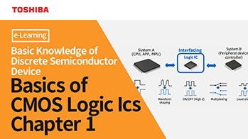
What are the differences among the general-purpose logic ICs?
General-purpose logic ICs (CMOS logic ICs/one-gate logic (L-MOS)) are made into series (family) based on operating voltage range, propagation delay time (speed), output current, input tolerance, etc.
These are often used for the purpose of signal conversion, distribution, switching, etc. in the control board of electronic equipment and the interface between boards.
The features of each series are as follows.
- Standard (TC40/TC45, TC4S/TC4W):
Covers a wide operating voltage range from 3 to 18 V and guarantees electrical characteristics at three supply voltages: 5 V, 10 V, and 15 V. - High speed (TC74HC/TC74HCT, TC7S/TC7W/TC7WT)
Widely used with a 5 V power supply - Advanced (TC74AC/TC74ACT)
Suitable as transmission line drivers because of high output current (24 mA) - Very High Speed (TC74VHC/74VHC/TC74VHCT/74VHCT/TC74VHCV/74VHCV, TC7SH/TC7WH/TC7PH/TC7SET)
Combines high speed and low noise; most widely used for applications requiring high-speed operations because of the highest speed at 5 V under light-load conditions - For low-voltage systems
Low voltage (TC74LCX/74LCX, TC7SZ/TC7PZ/TC7WZ)
Even at a VCC of 3.3 V, provides speed equivalent to the conventional 5 V high-speed series (AC/VHC series) and guarantees correct operation at 2.5 V and 1.8 V
Very low voltage (TC74VCX, 7UL).
The very low Voltage is a series that achieves even faster speeds and VCC = 1.2 V (7UL series is a series that guarantees operation with 0.9 V).
Type |
Series Name |
CMOS Logic ICs Series No. |
One-Gate Logic ( L-MOS ) Equivalent |
Operating Voltage Range VCC (V) |
Propagation |
Output Current *2 IOUT (mA) |
Input-Tolerant |
Output Power-down Protection |
|---|---|---|---|---|---|---|---|---|
For 5 V Systems |
Standard |
3 to 18 |
200 |
±0.51 |
△*3 |
- |
||
High Speed |
2 to 6 |
23 |
±4.0 or ±6.0 |
△*3 |
- |
|||
4.5 to 5.5 |
31 |
- | ||||||
Advanced |
2 to 5.5 |
8.5 |
±24 |
- |
- |
|||
4.5 to 5.5 |
9.0 |
|||||||
Very High Speed |
2 to 5.5 |
8.5 |
±8.0 |
● |
- |
|||
10 |
||||||||
4.5 to 5.5 |
9.5 |
● |
●*4 |
|||||
1.8 to 5.5 |
8.5 |
±16 |
● |
● |
||||
For low |
Low Voltage |
1.65 to 3.6 |
6.5 |
±24 |
● |
●*5 |
||
Very Low Voltage |
1.2 to 3.6 |
4.2 |
±24 |
● |
● |
*1: Maximum propagation delay time of typical ICs (TC4001, TC74HC244, TC74HCT244, TC74AC244, TC74ACT244, 74VHC244, 74VHC9541 (An-Yn), VHCT244, VHCV244, 74LCX244, and TC74VCX244) at -40 to 85 °C, except for the TC4001 for which the maximum propagation delay time at 25 °C is shown.
*2: Those output current values are from DC Characteristics table of the datasheet. In addition, they are specified in absolute maximum ratings.
*3: TC4049BF/BP, TC4050BF/BP, TC74HC4049BP/BF/BFT, 74HC4049D, TC74HC4050BP/BF/BFT and 74HC4050D have the input-tolerant function that allows level shifting from a higher voltage to a lower voltage.
*4: The TC7SET series and TC7SZU04/TC7WZU04 does not have an output power-down protection function.
*5: The TC7SZ series in the fSV package do not have an output power-down protection function except those with an open-drain output.
Related Links
The following documents also contain related information.