
- General Top
- SEMICONDUCTOR
- STORAGE
- COMPANY
-
My ToshibaSemicon
- Semiconductor Top
-
ApplicationsAutomotive
Body Electronics
xEV
In-Vehicle Infotainment
Advanced Driver-Assistance Systems (ADAS)
Chassis
IndustrialInfrastructure
BEMS/HEMS
Factory Automation
Commercial Equipment
Consumer/PersonalIoT Equipment
Healthcare
Wearable Device
Mobile
Computer Peripherals
-
ProductsAutomotive Devices
Discrete Semiconductor
Diodes
Transistors
Logic ICs
Analog Devices
- Automotive SmartMCD™ (Integreted SoC Conbining Microcontroller and Driver)
- Automotive Brushless Motor Driver ICs
- Automotive Brushed DC Motor Driver ICs
- Automotive Stepping Motor Driver ICs
- Automotive Driver ICs
- Automotive System Power Supplies ICs
- Automotive audio power amplifier ICs
- Automotive Network Communication
Digital Devices
Wireless Devices
※
 : Products list (parametric search)Power Semiconductors
SiC Power Devices
※
: Products list (parametric search)Isolators/Solid State RelaysPhotocouplers
Digital Isolators
Solid State Relays
Fiber Optic Transmitting Modules
※
: Products list (parametric search)MOSFETsIGBTs/IEGTsBipolar Transistors※
: Products list (parametric search)Diodes※
: Products list (parametric search)MicrocontrollersMotor Driver ICsIntelligent Power ICs※
: Products list (parametric search)Power Management ICsLinear ICs※
: Products list (parametric search)General Purpose Logic ICsLinear Image SensorsOther Product ICsOther Product ICs
※
: Products list (parametric search) -
Design & Development
-
Knowledge
- Where To Buy


- Part Number & Keyword Search
- Cross Reference Search
- Parametric Search
- Stock Check & Purchase
This webpage doesn't work with Internet Explorer. Please use the latest version of Google Chrome, Microsoft Edge, Mozilla Firefox or Safari.
require 3 characters or more. Search for multiple part numbers fromhere.
The information presented in this cross reference is based on TOSHIBA's selection criteria and should be treated as a suggestion only. Please carefully review the latest versions of all relevant information on the TOSHIBA products, including without limitation data sheets and validate all operating parameters of the TOSHIBA products to ensure that the suggested TOSHIBA products are truly compatible with your design and application.Please note that this cross reference is based on TOSHIBA's estimate of compatibility with other manufacturers' products, based on other manufacturers' published data, at the time the data was collected.TOSHIBA is not responsible for any incorrect or incomplete information. Information is subject to change at any time without notice.
require 3 characters or more.
Commercialization of new TO-247-4L packaging 600-V Super Junction Power MOSFET (DTMOSIV-H Series)
The four-pin TO-247-4L package, which uses Kelvin-connected signal-source terminals for gate drive, can reduce the effect of the inductances of the source wires inside the package, thereby further enhancing the high-speed switching performance of MOSFET chips.
This helps improve the efficiency of mid- and large-class high-efficiency switched-mode power supplies (equivalent to 80 PLUS of ※1 power TITANIUM/PLATINUM).
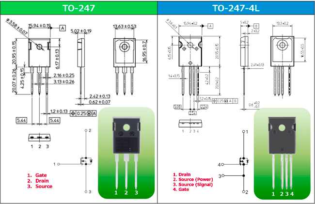
Advantages of TO-247-4L packages
As DTMOS speeds and currents increase, the inductance components of the source wires inside the package affect the high-speed switchability of the package. By providing the signal source terminal for the gate drive, the current in the power line and the current in the gate drive line can be separated to reduce the influence of the inductance of the gate-source voltage.
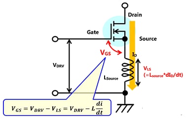
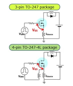
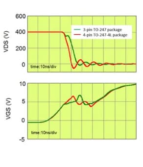
For >3-pin packages (TO-247)
The back electromotive voltage VLS (=LS*dID/dt) is generated by the inductance component L Source of the source wire and the slope dI dID/dt of the drain current of the voltage VGS applied between the gate and the source of the FET chip. The actual applied voltage is reduced from the set gate voltage by this back electromotive force, and the switching speed, especially turn-on, is slowed down.
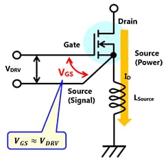
For >4-pin packages (TO-247-4L)
Moving the source terminal on the drive side from a location close to the FET chip separated from the source wire on the load side makes it less susceptible to the drive voltage. This makes it possible to improve the high-speed switching performance of the FET chip.
Reduction of turn-on losses by TO-247-4L
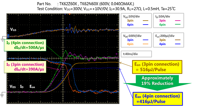
When we looked at the gate-source voltage waveforms in the immediate vicinity of MOSs, we confirmed that the on-time of TO-247-4L packages was shortened by the L Source. In the actual measurement, we confirmed that the turn-on loss of the TO-247-4L package (part number: TK62Z60X) was reduced by 19% compared with the turn-on loss of the TO-247 package (part number: TK62N60X).
Regarding the effect of reducing the turn-on loss, we confirmed that the switching speed was improved in both the simulation and the actual measurement.
TO-247-4L packaged MOSFETs
Related information
Queries about purchasing, sampling and IC reliability
Stock Check & Purchase
require 3 characters or more.
Through this website you are able to proceed to the website of our distributors ("Third Party Website") which is not under the control of Toshiba Corporation and its subsidiaries and affiliates (collectively "Toshiba"). The Third Party Website is made available to you as a convenience only and you agree to use the Third Party Website at your own risk. The link of the Third Party Website does not necessarily imply a recommendation or an endorsement by Toshiba of the Third Party Website. Please be aware that Toshiba is not responsible for any transaction done through the Third Party Website, and such transactions shall be subject to terms and conditions which may be provided in the Third Party Website.