
- General Top
- SEMICONDUCTOR
- STORAGE
- COMPANY
-
My ToshibaSemicon
- Semiconductor Top
-
ApplicationsAutomotive
Body Electronics
xEV
In-Vehicle Infotainment
Advanced Driver-Assistance Systems (ADAS)
Chassis
IndustrialInfrastructure
BEMS/HEMS
Factory Automation
Commercial Equipment
Consumer/PersonalIoT Equipment
Healthcare
Wearable Device
Mobile
Computer Peripherals
-
ProductsAutomotive Devices
Discrete Semiconductor
Diodes
Transistors
Logic ICs
Analog Devices
- Automotive SmartMCD™ (Integreted SoC Conbining Microcontroller and Driver)
- Automotive Brushless Motor Driver ICs
- Automotive Brushed DC Motor Driver ICs
- Automotive Stepping Motor Driver ICs
- Automotive Driver ICs
- Automotive System Power Supplies ICs
- Automotive audio power amplifier ICs
- Automotive Network Communication
Digital Devices
Wireless Devices
※
 : Products list (parametric search)Power Semiconductors
SiC Power Devices
※
: Products list (parametric search)Isolators/Solid State RelaysPhotocouplers
Digital Isolators
Solid State Relays
Fiber Optic Transmitting Modules
※
: Products list (parametric search)MOSFETsIGBTs/IEGTsBipolar Transistors※
: Products list (parametric search)Diodes※
: Products list (parametric search)MicrocontrollersMotor Driver ICsIntelligent Power ICs※
: Products list (parametric search)Power Management ICsLinear ICs※
: Products list (parametric search)General Purpose Logic ICsLinear Image SensorsOther Product ICsOther Product ICs
※
: Products list (parametric search) -
Design & Development
-
Knowledge
- Where To Buy


- Part Number & Keyword Search
- Cross Reference Search
- Parametric Search
- Stock Check & Purchase
This webpage doesn't work with Internet Explorer. Please use the latest version of Google Chrome, Microsoft Edge, Mozilla Firefox or Safari.
require 3 characters or more. Search for multiple part numbers fromhere.
The information presented in this cross reference is based on TOSHIBA's selection criteria and should be treated as a suggestion only. Please carefully review the latest versions of all relevant information on the TOSHIBA products, including without limitation data sheets and validate all operating parameters of the TOSHIBA products to ensure that the suggested TOSHIBA products are truly compatible with your design and application.Please note that this cross reference is based on TOSHIBA's estimate of compatibility with other manufacturers' products, based on other manufacturers' published data, at the time the data was collected.TOSHIBA is not responsible for any incorrect or incomplete information. Information is subject to change at any time without notice.
require 3 characters or more.
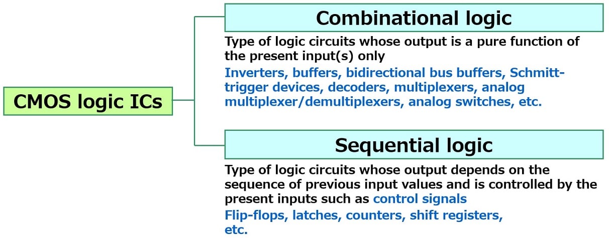
3-3-2. Sequential Logic: Flip-Flops
Flip-flops
Example: 74VHC74
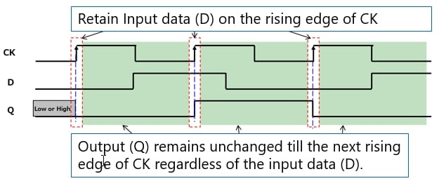
A flip-flop can retain data under specific conditions. The word “flip-flop” is sometimes abbreviated as FF. There are several types of flip-flops such as D-type and JK flip-flops. As an example, the following describes the operation of a D-type flip-flop.
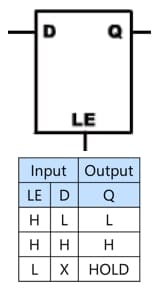
A D-type flip-flop differs from a D-type latch in that the D-type flip-flop retains output data even after the clock is set inactive (Low in this example). (A D-type latch transfers data from the D input to the Q output while the LE input is High.)
For example, a D-type flip-flop has an input data pin (D), a clock pin (CK), and an output data pin (Q). This flip-flop latches input data (D) on the rising edge of CK and transfers them to Q. Q remains unchanged till the next rising edge of CK regardless of the input data (D). In other words, Q retains the input data (D) latched on the previous rising edge of CK. The following shows the timing diagram of a D-type flip-flop. Some flip-flops have a clear (CLR) or preset (PR) input pin that is used to initialize the internal state to a known value.
Flip-flops are used for synchronizers for asynchronous signals and delay circuits for digital signals as well as counters, frequency dividers, etc.
Operation of a D-type flip-flop
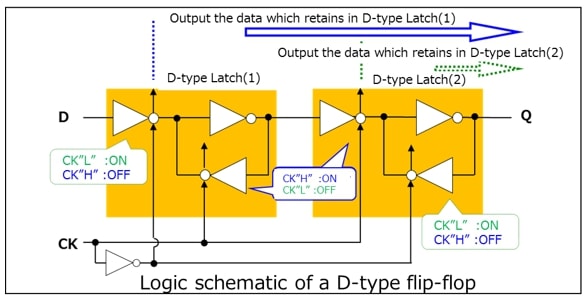
The following describes the operation of a D-type flip-flop using a logic schematic.
A D-type flip-flop consists of two D-type latches.
When a rising clock edge is applied to CK, D-type latch #1 is activated. While the clock (CK) is High, D-type latch #1 remains active, and thus the first clocked inverter in D-type Latch #2 is also active.
Therefore, the data held in D-type latch #1 are transferred to the output (Q) as highlighted by the blue arrow. The output remains unchanged even if the input changes state.
When a falling clock edge is applied to CK, D-type latch #2 is activated.
As a result, the data held in D-type latch #2 continue to appear at the output (Q) as highlighted by the green arrow. Again, the output remains unchanged even if the input changes state.
It should be noted that the value of the output (Q) is unknown until a known input is latched on the rising edge of the clock (CK).

Chapter3 Basic CMOS Logic ICs


Products
Related information
- Application Notes
- FAQ