
- General Top
- SEMICONDUCTOR
- STORAGE
- COMPANY
-
My ToshibaSemicon
- Semiconductor Top
-
ApplicationsAutomotive
Body Electronics
xEV
In-Vehicle Infotainment
Advanced Driver-Assistance Systems (ADAS)
Chassis
IndustrialInfrastructure
BEMS/HEMS
Factory Automation
Commercial Equipment
Consumer/PersonalIoT Equipment
Healthcare
Wearable Device
Mobile
Computer Peripherals
-
ProductsAutomotive Devices
Discrete Semiconductor
Diodes
Transistors
Logic ICs
Analog Devices
- Automotive SmartMCD™ (Integreted SoC Conbining Microcontroller and Driver)
- Automotive Brushless Motor Driver ICs
- Automotive Brushed DC Motor Driver ICs
- Automotive Stepping Motor Driver ICs
- Automotive Driver ICs
- Automotive System Power Supplies ICs
- Automotive audio power amplifier ICs
- Automotive Network Communication
Digital Devices
Wireless Devices
※
 : Products list (parametric search)Power Semiconductors
SiC Power Devices
※
: Products list (parametric search)Isolators/Solid State RelaysPhotocouplers
Digital Isolators
Solid State Relays
Fiber Optic Transmitting Modules
※
: Products list (parametric search)MOSFETsIGBTs/IEGTsBipolar Transistors※
: Products list (parametric search)Diodes※
: Products list (parametric search)MicrocontrollersMotor Driver ICsIntelligent Power ICs※
: Products list (parametric search)Power Management ICsLinear ICs※
: Products list (parametric search)General Purpose Logic ICsLinear Image SensorsOther Product ICsOther Product ICs
※
: Products list (parametric search) -
Design & Development
-
Knowledge
- Where To Buy


- Part Number & Keyword Search
- Cross Reference Search
- Parametric Search
- Stock Check & Purchase
This webpage doesn't work with Internet Explorer. Please use the latest version of Google Chrome, Microsoft Edge, Mozilla Firefox or Safari.
require 3 characters or more. Search for multiple part numbers fromhere.
The information presented in this cross reference is based on TOSHIBA's selection criteria and should be treated as a suggestion only. Please carefully review the latest versions of all relevant information on the TOSHIBA products, including without limitation data sheets and validate all operating parameters of the TOSHIBA products to ensure that the suggested TOSHIBA products are truly compatible with your design and application.Please note that this cross reference is based on TOSHIBA's estimate of compatibility with other manufacturers' products, based on other manufacturers' published data, at the time the data was collected.TOSHIBA is not responsible for any incorrect or incomplete information. Information is subject to change at any time without notice.
require 3 characters or more.
The device under protection (DUP) should not be degraded or destroyed in the event of an ESD strike
When ESD energy enters a circuit, an ESD protection diode turns on, shunting large current to GND. The voltage across the diode during an ESD event is defined as clamp voltage, VC. While the ESD protection diode is on, it can be regarded as being connected in parallel with the device under protection (DUP). It should be noted that a small amount of time is required for the ESD protection diode to turn on.
Therefore, ESD energy is applied to the DUP until the ESD protection diode turns on. Even after the ESD protection diode turns on, a voltage lower than its reverse breakdown voltage is applied to the DUP. The currents that flow to the ESD protection diode and the DUP are inversely proportional to their respective impedances. The impedance of the ESD protection diode during the “on” state is defined as dynamic resistance.
There are various types of ESD protection devices. ESD protection diodes have the following characteristics:
- Even low-capacitance diodes provide low dynamic resistance, which is a figure of merit for ESD protection.
- ESD protection diodes turn on quickly in the event of an ESD strike.
- ESD protection diodes do not deteriorate even after multiple ESD strikes.
Figure 5 compares the performance of three ESD protection diodes with different clamp voltage (VC) specifications, showing the voltage measured at the input of the DUP after an ESD entry. Figure 5 should be considered merely as a guide as these waveforms are the results of ESD application to a connector, not to the end of an antenna. Although the DF2B5M5SL and DF2B5M4SL provide similar clamp voltages (VC), their first peak voltages differ roughly by 50%.
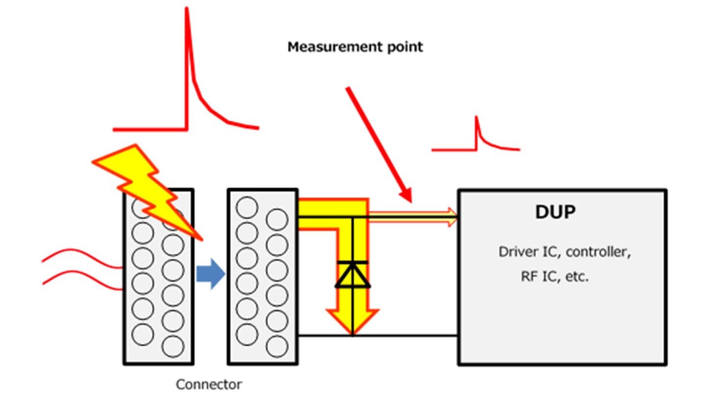
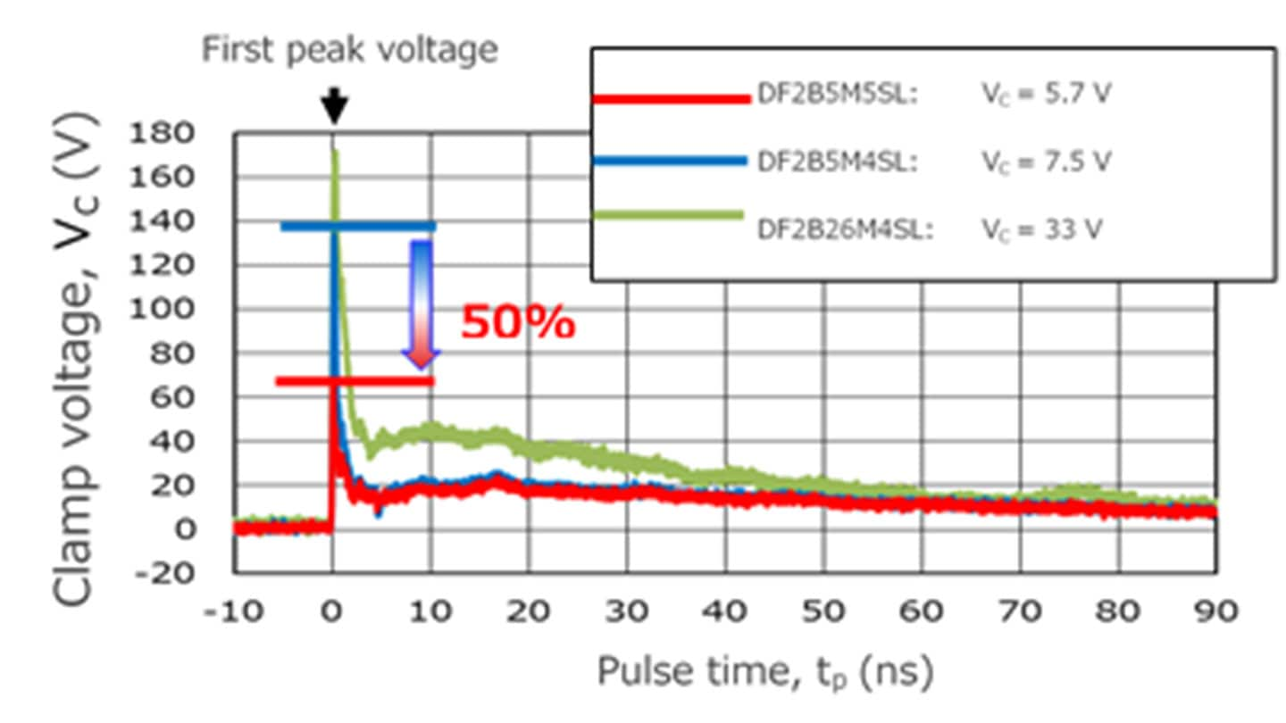
Figure 5 Effects of clamp voltage on ESD protection performance
(ESD protection diodes with different clamp voltage specifications)
The following are the considerations for preventing the degradation or destruction of the DUP:
- Select ESD protection diodes with low clamp voltage.
- Select ESD protection diodes with low reverse breakdown voltage (VBR) or working peak reverse voltage.
- Select ESD protection diodes with low dynamic resistance.
The second requirement above contradicts the third requirement described in Section 1 (VRWM higher than the maximum signal amplitude). In order to enhance the overall ESD tolerance of a system, check the ESD tolerance of the RF IC and select an ESD protection diode capable of absorbing ESD energy exceeding the ESD tolerance.