
- General Top
- SEMICONDUCTOR
- STORAGE
- COMPANY
-
My ToshibaSemicon
- Semiconductor Top
-
ApplicationsAutomotive
Body Electronics
xEV
In-Vehicle Infotainment
Advanced Driver-Assistance Systems (ADAS)
Chassis
IndustrialInfrastructure
BEMS/HEMS
Factory Automation
Commercial Equipment
Consumer/PersonalIoT Equipment
Healthcare
Wearable Device
Mobile
Computer Peripherals
-
ProductsAutomotive Devices
Discrete Semiconductor
Diodes
Transistors
Logic ICs
Analog Devices
- Automotive SmartMCD™ (Integreted SoC Conbining Microcontroller and Driver)
- Automotive Brushless Motor Driver ICs
- Automotive Brushed DC Motor Driver ICs
- Automotive Stepping Motor Driver ICs
- Automotive Driver ICs
- Automotive System Power Supplies ICs
- Automotive audio power amplifier ICs
- Automotive Network Communication
Digital Devices
Wireless Devices
※
 : Products list (parametric search)Power Semiconductors
SiC Power Devices
※
: Products list (parametric search)Isolators/Solid State RelaysPhotocouplers
Digital Isolators
Solid State Relays
Fiber Optic Transmitting Modules
※
: Products list (parametric search)MOSFETsIGBTs/IEGTsBipolar Transistors※
: Products list (parametric search)Diodes※
: Products list (parametric search)MicrocontrollersMotor Driver ICsIntelligent Power ICs※
: Products list (parametric search)Power Management ICsLinear ICs※
: Products list (parametric search)General Purpose Logic ICsLinear Image SensorsOther Product ICsOther Product ICs
※
: Products list (parametric search) -
Design & Development
-
Knowledge
- Where To Buy


- Part Number & Keyword Search
- Cross Reference Search
- Parametric Search
- Stock Check & Purchase
This webpage doesn't work with Internet Explorer. Please use the latest version of Google Chrome, Microsoft Edge, Mozilla Firefox or Safari.
require 3 characters or more. Search for multiple part numbers fromhere.
The information presented in this cross reference is based on TOSHIBA's selection criteria and should be treated as a suggestion only. Please carefully review the latest versions of all relevant information on the TOSHIBA products, including without limitation data sheets and validate all operating parameters of the TOSHIBA products to ensure that the suggested TOSHIBA products are truly compatible with your design and application.Please note that this cross reference is based on TOSHIBA's estimate of compatibility with other manufacturers' products, based on other manufacturers' published data, at the time the data was collected.TOSHIBA is not responsible for any incorrect or incomplete information. Information is subject to change at any time without notice.
require 3 characters or more.
Compact and Low-Noise LDO Regulators that Provide Fast Response from Standby to Stabilize DC Power Line
Toshiba Electronic Devices & Storage Corporation ("Toshiba") has launched the TCR5FM series of 35 LDO regulators, which help stabilize the DC power line for small equipment, such as mobile devices and wearable devices.
In recent years, wearable devices have been expected to deliver high performance while maintaining long battery life. This has led to a trend of alternating between low-power operation and high-speed processing. Switching between these operating modes can destabilize the power supply line. Therefore, LDO regulators that contribute to stabilizing DC power line are in demand.
The new TCR5FM series improves load transient response from standby by approximately 80%[1] compared to Toshiba’s existing product, the TCR3RM series, by quickly detecting fluctuations in output voltage and providing fast feedback. As a result, even during sudden load changes, variations in output voltage are reduced. The TCR5FM series features a high ripple rejection ratio[2] of 91dB (typ.)[3], which is top class in the industry[4], achieved by combining a bandgap circuit, a low-pass filter[5], and a high-speed, low-noise operational amplifier. This enhances noise rejection capability and enables the output of a low-noise voltage. Due to these features, the new TCR5FM series helps stabilize DC power lines and is suitable for noise-sensitive applications such as CMOS sensors and power supplies for high-frequency circuits.
The maximum output current is 500mA and operating temperature range supports up to 125°C. The line-up includes 35 products, and the output voltages range from 0.9V to 5.0V, allowing users to select the output voltage suited to their applications.
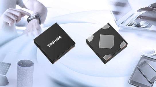
The package is a small DFN4D package, 1mm×1mm, suitable for mobile devices and wearable devices requiring high-density mounting.
Toshiba will continue to expand its lineup of LDO regulator series and promote product development to meet diverse customer needs.
Notes:
[1] Values measured by Toshiba. Test condition: VIN=3.3V, VOUT=2.8V, IOUT=0mA ⇔ 100mA, tr=1.0μs, tf=1.0μs, Ta=25°C
[2] Ripple rejection ratio, also referred to as PSRR (Power Supply Rejection Ratio), is a quantitative index that indicates how much ripple voltage component (noise) superimposed on the input voltage is transmitted to the output voltage. It is expressed as the ratio between the input ripple voltage and the resulting output ripple voltage.
[3] Values measured by Toshiba. Test condition: CIN=none, COUT=1.0μF, VIN=3.3V, VOUT=2.8V, VIN Ripple=200mVp-p, IOUT=10mA, Ta=25°C
[4] Among LDO regulators with a maximum output of 500mA, Toshiba surveyed as of October 2025.
[5] A filter that allows only low-frequency components to pass through while blocking high-frequency components.
Features
- Fast load transient response: ΔVOUT=-75/+25mV (typ.) (IOUT=0mA ⇔ 100mA, VOUT=2.8V)
- High ripple rejection ratio: R.R.=91dB (typ.) (f=1kHz, VOUT=2.8V)
- Low output noise voltage: VNO=5μVrms (typ.) (10Hz≦f≦100kHz)
Features Explanation
1. Fast load transient response: ΔVOUT=-75/+25mV (typ.) (IOUT=0mA ⇔ 100mA, VOUT=2.8V)
The TCR5FM series offers fast response performance to sudden load changes. Compared to Toshiba’s existing product, the TCR3RM series, the response from no-load conditions (standby) has improved by approximately 80%[1], with a typical load transient response of -75mV/+25mV at 2.8V output for a 0mA ⇔ 100mA load change. It also delivers excellent response under loaded conditions, with a typical load transient response of -60mV/+40mV at 2.8V output for a 1mA ⇔ 500mA load change. This contributes to the stable operation of the downstream circuit.
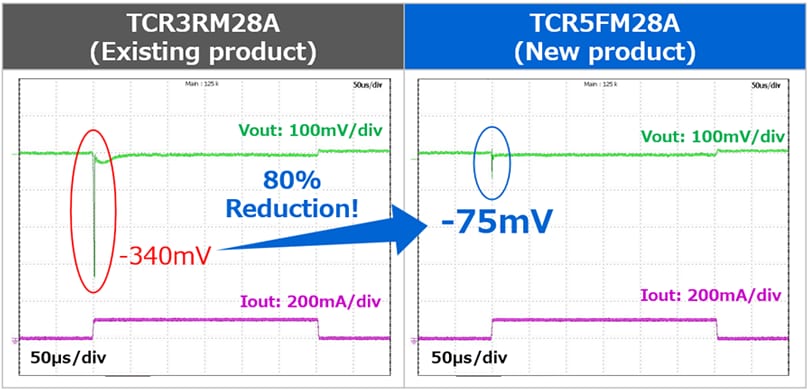
Figure 1. Comparison of Load Transient Response Characteristics between Existing and New Products
(VIN=3.3V, VOUT=2.8V, IOUT=0mA ⇔ 100mA, tr=1.0μs, tf=1.0μs, Ta=25°C)
2. High ripple rejection ratio: R.R.=91dB (typ.) (f=1kHz, VOUT=2.8V)
The ripple rejection ratio indicates the ratio between the ripple voltage component superimposed on the input voltage and the ripple voltage that appears on the output voltage. The TCR5FM series achieves high ripple rejection by combining a bandgap circuit, a low-pass filter[5], and a high-speed, low-noise operational amplifier. The TCR5FM series delivers top class performance in the industry[4], with a ripple rejection ratio of 91dB (typ.) (f=1kHz) using a 3.3V input and 2.8V output. This enables low-noise output.
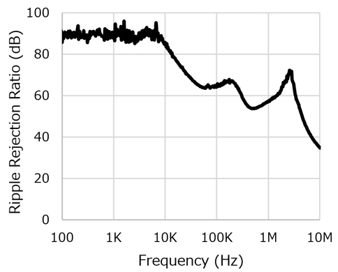
Figure 2. Characteristic of ripple compression ratio
(CIN=none, COUT=1.0μF, VIN=3.3V, VOUT=2.8V, VIN Ripple=200mVp-p, IOUT=10mA, Ta=25°C)
3. Low output noise voltage: VNO=5μVrms (typ.) (10Hz≦f≦100kHz)
Output noise voltage refers to the integrated value of noise occurring in the output voltage of the LDO. TCR5FM series features industry-leading[2] performance, 5μVrms (typ.) (10Hz≦f≦100kHz) with 3.3V input, 2.8V output. This allows for low-noise output. The new TCR5FM series is suitable for noise-sensitive applications such as high-sensitivity analog circuits, RF circuits, and sensor power supplies.
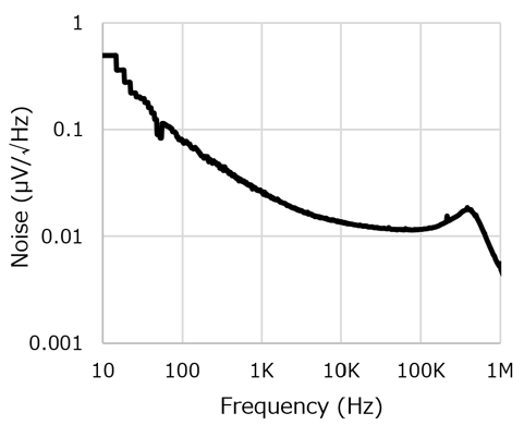
Figure 3. Characteristic of output noise
(CIN=1.0μF, COUT=1.0μF, VIN=3.3V, VOUT=2.8V, IOUT=10mA, Ta=25°C)
Applications
- Mobile devices, wearable devices, IoT devices, etc.
Main Specifications
| Part number | TCR5FM series | ||
|---|---|---|---|
| Package | Name | DFN4D | |
| Size (mm) | Typ. | 1.0×1.0, t=0.37 | |
| Operating range (Topr=-40 to 125°C) |
Output current IOUT (mA) | 500 | |
| Input voltage VIN (V) | 1.55 to 5.5[6] | ||
| Output voltage VOUT (V) | 0.9 to 5.0 | ||
| Electrical characteristics (Unless otherwise specified, Tj=25°C) |
Quiescent current IB(ON) (µA) IOUT=0mA[7] |
Typ. | 10 |
| Max | 20[8] | ||
| Drop-out voltage VDO (mV)[9] IOUT=500mA, VOUT=2.8V |
Typ. | 220 | |
| Max | 337[8] | ||
| Load transient response ⊿VOUT (mV) IOUT=1mA ⇔ 500mA, VOUT=2.8V |
Typ. | -60/+40 | |
| Load transient response ⊿VOUT (mV) IOUT=0mA ⇔ 100mA, VOUT=2.8V |
Typ. | -75/+25 | |
| Ripple rejection ratio R.R. (dB) f=1kHz, IOUT=10mA, VOUT=2.8V |
Typ. | 91 | |
| Output noise voltage VNO (µVrms) VOUT=2.8V, IOUT=10mA, 10Hz≦f≦100kHz |
Typ. | 5 | |
| Control pin voltage (HIGH) VCTH (V) | Min | 0.79[8] | |
| Control pin voltage (LOW) VCTL (V) | Max | 0.4[8] | |
| Sample check & availability |  |
||
Notes:
[6] Please refer to the dropout voltage table for each output voltage listed in the datasheet and use within the absolute maximum junction temperature and operating temperature ranges.
[7] Control terminal current (ICT) is not included.
[8] Tj=-40 to 125°C
[9] VDO=VIN1-(VOUT1×0.97)
VOUT1 is the output voltage when VIN=VOUT+0.5V.
VIN1 is the input voltage at which the output voltage becomes 97% of VOUT1 after gradually decreasing the input voltage.
Related information
Product information
Low-Dropout Regulators
Technical articles
Noise reduction due to high ripple rejection ratio
LDO Regulators: Fast load transient response performance
LDO Regulators: Reduction of power consumption by low dropout voltage
Application notes
Basics of Low-Dropout (LDO) Regulator ICs (PDF: 1.3MB)
Concept of self-heating of LDOs and selection guide (PDF: 767KB)
Load Transient Response of LDO and Methods to Improve it (PDF: 1.2MB)
Simple Guide to Improving Ripple Rejection Ratio of LDO Regulators (PDF: 1.3MB)
Application examples of LDO regulators with high ripple rejection and fast load transient response (PDF: 684KB)
Applications
Wireless Earbuds
Smart Watch
IoT Sensor
Surveillance Camera
Solid State Drive
FAQ
LDO Regulators
Queries about purchasing, sampling and IC reliability
Stock Check & Purchase
require 3 characters or more.
Through this website you are able to proceed to the website of our distributors ("Third Party Website") which is not under the control of Toshiba Corporation and its subsidiaries and affiliates (collectively "Toshiba"). The Third Party Website is made available to you as a convenience only and you agree to use the Third Party Website at your own risk. The link of the Third Party Website does not necessarily imply a recommendation or an endorsement by Toshiba of the Third Party Website. Please be aware that Toshiba is not responsible for any transaction done through the Third Party Website, and such transactions shall be subject to terms and conditions which may be provided in the Third Party Website.
* Company names, product names, and service names may be trademarks of their respective companies.
* Information in this document, including product prices and specifications, content of services and contact information, is current on the date of the announcement but is subject to change without prior notice.