
- General Top
- SEMICONDUCTOR
- STORAGE
- COMPANY
-
My ToshibaSemicon
- Semiconductor Top
-
ApplicationsAutomotive
Body Electronics
xEV
In-Vehicle Infotainment
Advanced Driver-Assistance Systems (ADAS)
Chassis
IndustrialInfrastructure
BEMS/HEMS
Factory Automation
Commercial Equipment
Consumer/PersonalIoT Equipment
Healthcare
Wearable Device
Mobile
Computer Peripherals
-
ProductsAutomotive Devices
Discrete Semiconductor
Diodes
Transistors
Logic ICs
Analog Devices
- Automotive SmartMCD™ (Integreted SoC Conbining Microcontroller and Driver)
- Automotive Brushless Motor Driver ICs
- Automotive Brushed DC Motor Driver ICs
- Automotive Stepping Motor Driver ICs
- Automotive Driver ICs
- Automotive System Power Supplies ICs
- Automotive audio power amplifier ICs
- Automotive Network Communication
Digital Devices
Wireless Devices
※
 : Products list (parametric search)Power Semiconductors
SiC Power Devices
※
: Products list (parametric search)Isolators/Solid State RelaysPhotocouplers
Digital Isolators
Solid State Relays
Fiber Optic Transmitting Modules
※
: Products list (parametric search)MOSFETsIGBTs/IEGTsBipolar Transistors※
: Products list (parametric search)Diodes※
: Products list (parametric search)MicrocontrollersMotor Driver ICsIntelligent Power ICs※
: Products list (parametric search)Power Management ICsLinear ICs※
: Products list (parametric search)General Purpose Logic ICsLinear Image SensorsOther Product ICsOther Product ICs
※
: Products list (parametric search) -
Design & Development
-
Knowledge
- Where To Buy


- Part Number & Keyword Search
- Cross Reference Search
- Parametric Search
- Stock Check & Purchase
This webpage doesn't work with Internet Explorer. Please use the latest version of Google Chrome, Microsoft Edge, Mozilla Firefox or Safari.
require 3 characters or more. Search for multiple part numbers fromhere.
The information presented in this cross reference is based on TOSHIBA's selection criteria and should be treated as a suggestion only. Please carefully review the latest versions of all relevant information on the TOSHIBA products, including without limitation data sheets and validate all operating parameters of the TOSHIBA products to ensure that the suggested TOSHIBA products are truly compatible with your design and application.Please note that this cross reference is based on TOSHIBA's estimate of compatibility with other manufacturers' products, based on other manufacturers' published data, at the time the data was collected.TOSHIBA is not responsible for any incorrect or incomplete information. Information is subject to change at any time without notice.
require 3 characters or more.
3-5. Noise gain and signal gain
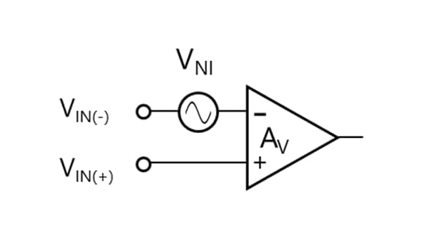
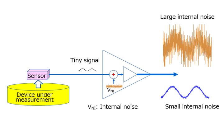
The previous section described different types of noise generated by the op-amp. As discussed, the internal noise of an op-amp is defined as equivalent input noise voltage. Figure 3-12 shows a simplified equivalent circuit. The op-amp represented by the triangle is the ideal one. Since Figure 3-12 expresses the equivalent input noise voltage (VNI) as a difference in voltage between VIN(+) and VIN(-), it is not significant whether VNI is inserted in series with VIN(+) or VIN(-).
Next, let’s consider noninverting and inverting amplifiers using this model.
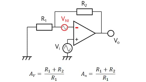
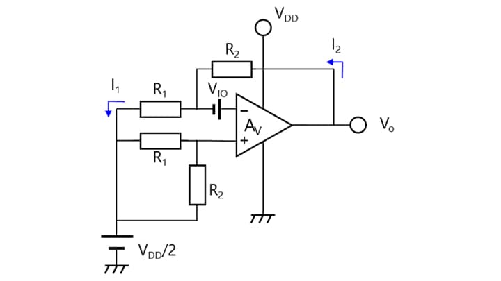
Figure 3-13 shows an inverting amplifier, and Figure 3-14 shows a noninverting amplifier. Both the inverting and noninverting amplifiers have an equivalent input noise source (VNI) inserted in series with the Vin(-) input of the ideal op-amp. These amplifiers have a signal gain of AV as discussed in Sections 2.4 and 2.5.

Using the principle of superposition, signal and noise sources can be considered separately. Let’s calculate the gain for the noise source. At this time, Vi is regarded as being short-circuited according to the principle of superposition.
Since the VIN(+) input is grounded in Figure 3-13, the VIN(-) input can also be regarded as being grounded. Therefore, the potential at the intersection of R1 and R2 becomes VNI.
Since the current flowing through R1 (I1) does not flow to the op-amp, all of I1 flows through R2.
I1 = VNI / R1
Hence, the noise voltage at VO (VNO) is calculated as:
VNO = VNI + R2 × VNI / R1 = VNI × (1 + R2 / R1)
Since the noise gain (AN) is equal to VNO/VNI,
AN = 1 + R2 / R1
In this way, the gain of the noise generated in an op-amp might be different from that of the signal gain. This gain is called a noise gain.
This concept of noise gain can be used as follows:
- Converting the equivalent input noise into output noise
- Calculating the effect of the input offset voltage on the output
- Calculating the oscillation margin
As described above, the concept of noise gain is important for circuits using an op-amp.
Next, the following paragraphs briefly describe the oscillation margin.
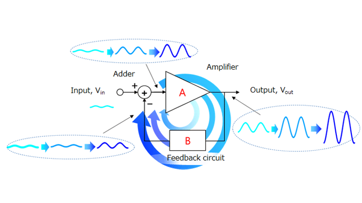
Except for oscillators, oscillation means an unwanted fluctuation of a signal at an unintended frequency. A source of oscillation such as unwanted noise circulates through a feedback loop, developing into oscillation, as described in Section 2.3.
The source of oscillation is random noise. It is applied as a difference in voltage between the VIN(+) and VIN(-) inputs of an op-amp. In other words, it is the equivalent input noise voltage (VNI) discussed above.
It is important to determine the oscillation immunity based on the noise gain. As described above, the noise gain of typical inverting and noninverting amplifiers can be calculated using the signal gain equation for noninverting amplifiers.
The concept of the noise gain can be used to provide a margin for oscillation (i.e., increase the noise gain).
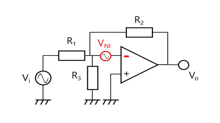
Figure 3-16 shows an example of increasing the oscillation margin without changing the signal gain with an inverting amplifier.
Let’s consider Vi and VNI separately using the principle of superposition.
(VNI is regarded as being short-circuited when considering Vi whereas Vi is regarded as being short-circuited when considering VNI.)
From the concept of a virtual short, both the VIN(-) and VIN(+) inputs are regarded as being grounded.
Therefore, since the voltage across R3 is equal to the GND potential at a signal gain of AV (= Vo/Vi), no current flows through R3. Hence, AV = -R2/R1, which is identical to the equation for a basic inverting amplifier.
Since Vi is short-circuited at a noise gain of AN (= Vo/VNI), Vi = R1 // R3. Hence, AN = 1 + R2 / (R1 // R3), which is higher than the noise gain for basic inverting amplifiers, AN = 1 + R2 / R1. This means that this circuit provides a larger oscillation margin than a basic inverting amplifier.
However, since the concept of the noise gain is exactly the same as that of the input offset voltage, the oscillation margin increases at the expense of an increase in input offset voltage.
Related information
Chapter3 Electrical characteristics
Related information
- Products
- Application Notes
- FAQs
- Parametric Search
- Stock Check & Purchase