- General Top
- SEMICONDUCTOR
- STORAGE
- COMPANY
-
My ToshibaSemicon
- Semiconductor Top
-
ApplicationsAutomotive
Body Electronics
xEV
In-Vehicle Infotainment
Advanced Driver-Assistance Systems (ADAS)
Chassis
IndustrialInfrastructure
BEMS/HEMS
Factory Automation
Commercial Equipment
Consumer/PersonalIoT Equipment
Healthcare
Wearable Device
Mobile
Computer Peripherals
-
ProductsAutomotive Devices
Discrete Semiconductor
Diodes
Transistors
Logic ICs
Analog Devices
- Automotive SmartMCD™ (Integreted SoC Conbining Microcontroller and Driver)
- Automotive Brushless Motor Driver ICs
- Automotive Brushed DC Motor Driver ICs
- Automotive Stepping Motor Driver ICs
- Automotive Driver ICs
- Automotive System Power Supplies ICs
- Automotive audio power amplifier ICs
- Automotive Network Communication
Digital Devices
Wireless Devices
※
 : Products list (parametric search)Power Semiconductors
SiC Power Devices
※
: Products list (parametric search)Isolators/Solid State RelaysPhotocouplers
Digital Isolators
Solid State Relays
Fiber Optic Transmitting Modules
※
: Products list (parametric search)MOSFETsIGBTs/IEGTsBipolar Transistors※
: Products list (parametric search)Diodes※
: Products list (parametric search)MicrocontrollersMotor Driver ICsIntelligent Power ICs※
: Products list (parametric search)Power Management ICsLinear ICs※
: Products list (parametric search)General Purpose Logic ICsLinear Image SensorsOther Product ICsOther Product ICs
※
: Products list (parametric search) -
Design & Development
-
Knowledge
- Where To Buy


- Part Number & Keyword Search
- Cross Reference Search
- Parametric Search
- Stock Check & Purchase
This webpage doesn't work with Internet Explorer. Please use the latest version of Google Chrome, Microsoft Edge, Mozilla Firefox or Safari.
require 3 characters or more. Search for multiple part numbers fromhere.
The information presented in this cross reference is based on TOSHIBA's selection criteria and should be treated as a suggestion only. Please carefully review the latest versions of all relevant information on the TOSHIBA products, including without limitation data sheets and validate all operating parameters of the TOSHIBA products to ensure that the suggested TOSHIBA products are truly compatible with your design and application.Please note that this cross reference is based on TOSHIBA's estimate of compatibility with other manufacturers' products, based on other manufacturers' published data, at the time the data was collected.TOSHIBA is not responsible for any incorrect or incomplete information. Information is subject to change at any time without notice.
require 3 characters or more.
What electrical characteristics are specified in the diode technical datasheets?
The main electrical characteristics specified in the diode datasheet are forward voltage, reverse current, terminal capacitance, reverse recovery time, etc.
This section describes each of the electrical characteristics specified in diode datasheets. Different electrical characteristics may be specified for different types of diodes. Electrical characteristics are specified at an ambient temperature (Ta) of 25°C unless otherwise noted.
An example of an electrical characteristic item in a diode technical datasheet is shown below.
| Characteristic | Symbol | Test Condition | Min | Typ. | Max | Unit |
|---|---|---|---|---|---|---|
| Forward voltage | VF (1) | IF = 1 mA | — | 0.61 | — | V |
| VF (2) | IF = 10 mA | — | 0.74 | — | ||
| VF (3) | IF = 100 mA | — | 0.92 | 1.20 | ||
| Reverse current | IR (1) | VR = 30 V | — | — | 0.1 | µA |
| IR (2) | VR = 80 V | — | — | 0.5 | ||
| Total capacitance | CT | VR = 0 V, f = 1 MHz | — | 2.2 | 4.0 | pF |
| Reverse recovery time | trr | IF = 10 mA (Fig. 1) | — | 1.6 | 4.0 | ns |
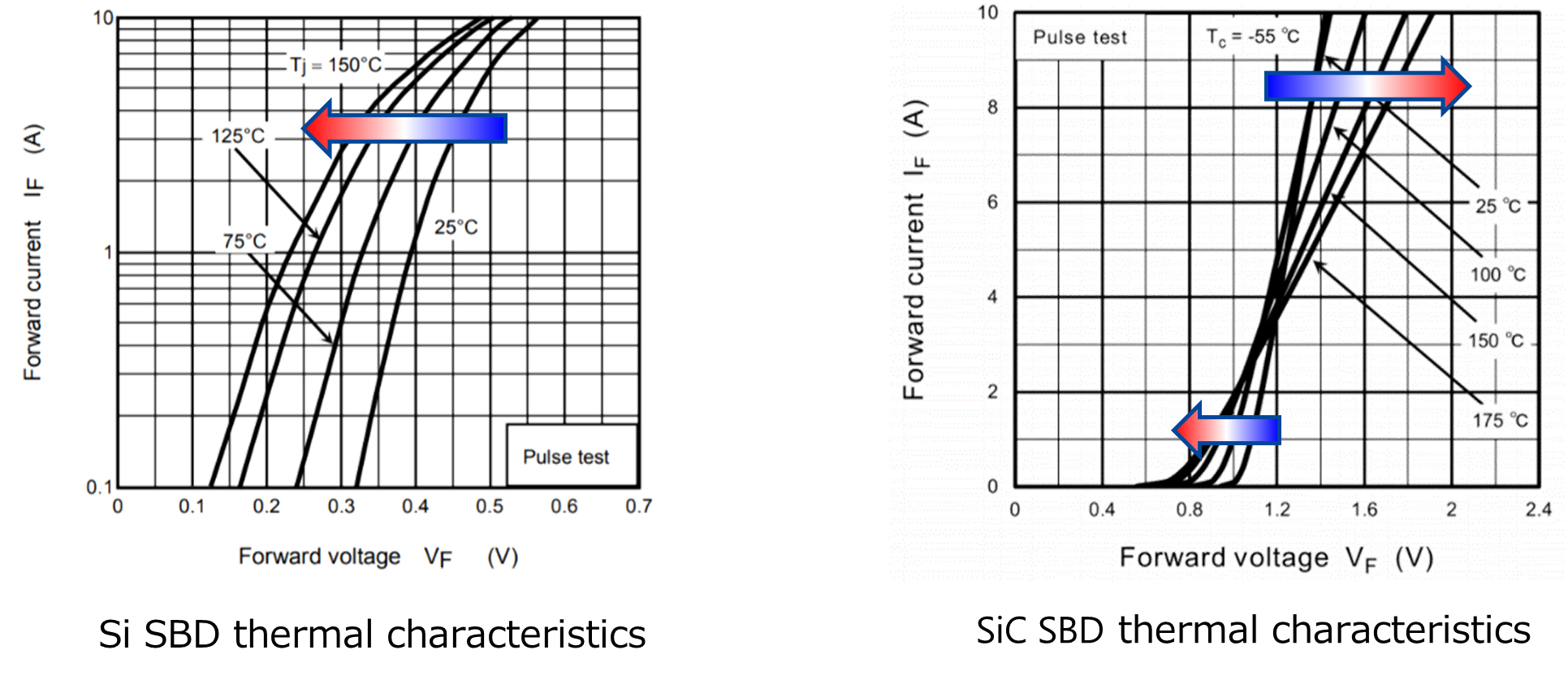
- Forward voltage (VF) / peak forward voltage (VFM)
VF and VFM are voltage drop that occur across a diode’s terminals when electric current flows in the forward direction under the specified current and temperature conditions. This is called forward voltage VF. Since VF and VFM are highly dependent on temperature, they are specified under a pulsed current condition for some diodes. In this case we call it the peak forward voltage VFM.
Generally, silicon SBDs have a negative temperature coefficient whereas SiC SBDs have a positive temperature coefficient in the high-current region. Therefore, parallel connection of Si diodes is not recommended due to the risk of thermal runaway.
The following FAQ has an explanation about temperature characteristics. please refer.
FAQ:How does heat change the characteristics of a diode? (Temperature Characteristic)
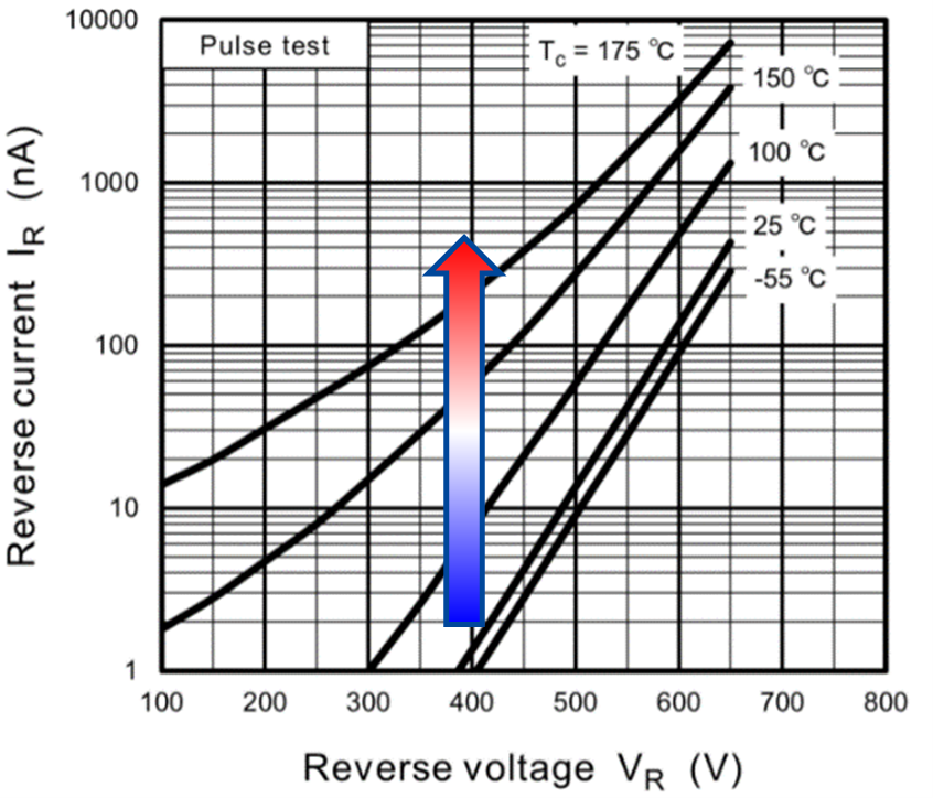
- Reverse current (IR) / repetitive peak reverse current (IRRM)
IR and IRRM are the leakage currents that flow in the reverse direction when a diode is reverse-biased at the specified voltage. Since the leakage currents are highly dependent on temperature, they are specified under a pulsed current condition for some diodes. Note that IR and IRRM are different from the maximum reverse recovery current observed during the reverse recovery process.
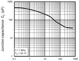
- Junction capacitance (Cj) / total capacitance (CT)
The main capacitance is the capacitance generated at the junction. There is a depletion layer at the junction, and there are almost no carriers (electrons or holes). This part corresponds to the insulation band of the capacitor. Since the width of the depletion layer is related to the magnitude of the applied reverse bias VR, the junction capacitance is inversely related to VR.
In the datasheet, Cj and CT are defined as the equivalent capacitance between the terminals when a small signal with the specified frequency is applied under the specified reverse voltage condition.
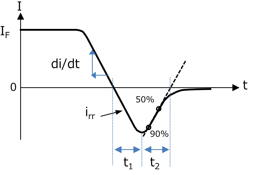
- Reverse recovery time (trr)
It takes some time to bring a forward-conducting diode into a non-conducting state by applying a reverse voltage. When forward voltage is applied across a pn junction diode, electrons are injected into the n-type semiconductor (i.e., cathode side) while holes are injected into the p-type semiconductor (i.e., anode side). These majority carriers recombine near the junction or diffuse across the junction as minority carriers, causing electric current to flow.
When reverse voltage is applied, negative current (i.e., reverse recovery current, irr) flows first, canceling out these majority carriers. Some of the minority carriers remaining in each layer recombine and disappear after a certain period of time (lifetime) has passed.
Reverse recovery time (trr) is the time required for reverse recovery current (irr) to disappear. In datasheets, trr is specified as follows. Forward current (IF) and its falling slew rate (di/dt) after the application of reverse voltage (VR) are specified as test conditions. Let the time required for IF to reach the peak value of the reverse recovery current (irr) value from the zero-crossing point be t1. Let the time required from the peak irr value to the zero-crossing point of the line passing through the 90% and 50% points of irr be t2. Then, reverse recovery time (trr) is defined as the sum of t1 and t2.
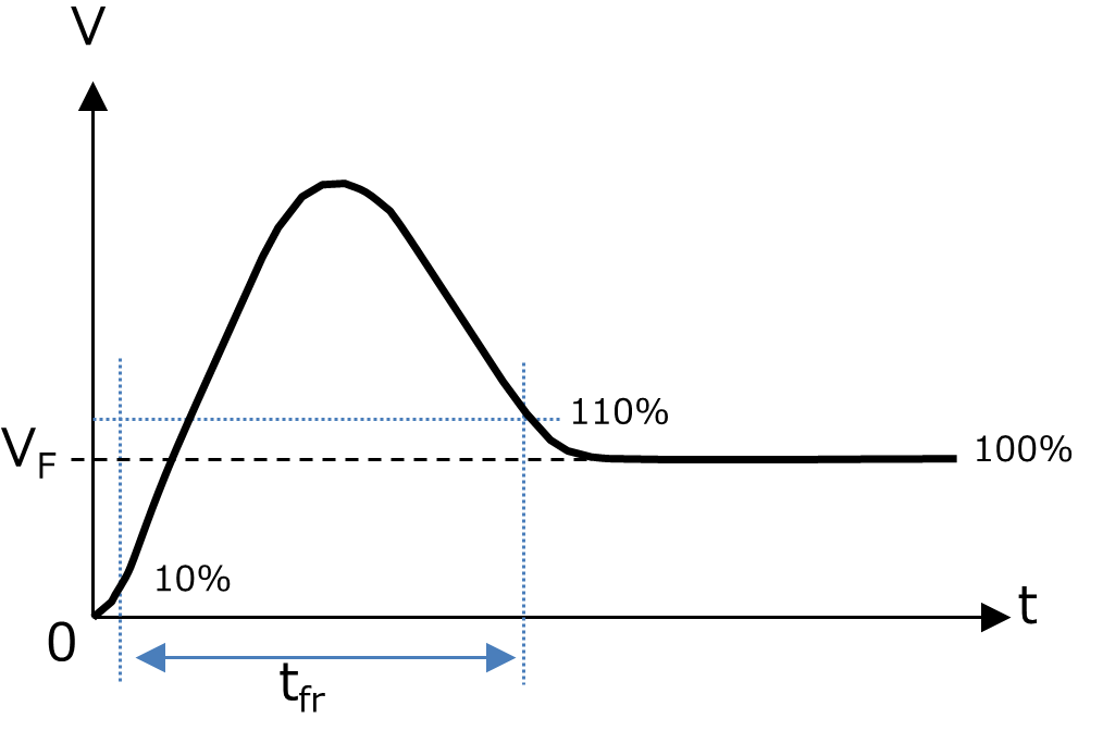
- Forward recovery time (tfr)
When a rapidly rising forward volta Even if a rapidly rising forward voltage is applied, the diode does not immediately become conductive. It takes a little time for enough carriers to be accumulated before the diode obtains high conductivity. Although the diode is forward-biased, it exhibits high resistance during this period and therefore a higher voltage than the VF value in the conducting state. This phenomenon is called forward recovery. A diode consumes more power during the forward recovery period than it does in the steady state.
In datasheets, tfr is defined as the time required for forward voltage to reach its peak from 10% of VF and then drop to 110% of VF at the specified forward current (IF). High-voltage diodes tend to have a long forward recovery time.
In addition, some diodes have individual maximum ratings. See the application note below for details.
Related Links
For products, please refer to the following links.