Bipolar Junction Transistor (BJT) Operation — Why Can a Small Current Control a Larger Current? (Active vs. Saturation Regions Explained)
A bipolar junction transistor (BJT) is widely known as a device in which the collector current (IC) can be controlled by the base current (IB) in the active region. However, this relationship does not mean that the base current directly determines the collector current. In reality, this current control relationship is established by the transport of carriers (electrons and holes) inside the transistor. When the conditions for carrier transport change, the proportional relationship between the base current and the collector current no longer holds. As a result, the transistor does not operate as an amplifying device and instead behaves as a switch.
Therefore, the operation of a BJT should be understood not simply as a current control relationship, but as a physical phenomenon governed by internal carrier transport conditions.
In this document, we focus on carrier transport processes such as diffusion, extraction (removal), storage, and recombination, and explain the differences in operation between the active region and the saturation region.
Specifically, the following topics are covered:
What you will learn
- Why the collector current is proportional to the base current in the active region
- Why this proportional relationship breaks down in the saturation region and the current gain (hFE) loses its meaning
- Why the saturation region is treated as the ON state of a switching device
These topics are explained by relating carrier transport processes to external circuit conditions.
For simplicity, the explanations are based on an NPN transistor. The same principles also apply to PNP transistors by reversing the polarity.
1. Overview of Bipolar Junction Transistors
A bipolar junction transistor (BJT) is a semiconductor device in which a current begins to flow when the base–emitter junction is forward biased while the collector is held at a higher potential than the emitter. The collector current varies with the base current. This state is referred to as the ON state.
The ON state can be divided into the active region and the saturation region depending on the operating conditions. In contrast, when no current flows, the device is in the OFF state, which is called the cutoff region.
Active Region
In the active region, the base–emitter junction is forward biased and the collector–base junction is reverse biased. Under this condition, the collector current changes approximately in proportion to the base current.
As a result, the current gain hFE is high and remains nearly constant, and the transistor operates as a current amplifier.
Saturation Region
When the external circuit sufficiently pulls down the collector voltage (VCE), the collector–base junction also becomes forward biased, and the transistor enters the saturation region.
In this state, the proportional relationship between base current and collector current observed in the active region breaks down. The apparent current gain hFE decreases, and it loses its validity as an indicator of current controllability.
Therefore, the transistor operates not as an amplifier but as a switch in the "ON" state.
Cutoff Region
In the cutoff region, the base–emitter junction is not forward biased, so almost no base current flows. As a result, the collector current is also nearly zero.
This state is referred to as the OFF state.
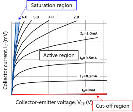
Fig. 1 : Operating regions of a bipolar junction transistor (active, saturation, cutoff)
2. Mechanism of Current Amplification in the Active Region
In the active region, the base–emitter (B–E) junction is forward biased and the base–collector (B–C) junction is reverse biased. Under these conditions, electrons are injected from the emitter into the base.
Due to the forward bias of the B–E junction, the electron concentration near the emitter side of the base becomes high. On the other hand, since the B–C junction is reverse biased, electrons are rapidly swept out by the electric field in the depletion region, and the electron concentration remains low near the collector side.
As a result, a concentration gradient is formed across the base region. This gradient drives diffusion, transporting electrons toward the collector. When electrons reach the depletion region, they are immediately accelerated by the electric field and are efficiently collected by the collector.
Thus, current amplification is established through the sequence of processes:
injection → diffusion transport → collection
2-1. Electron Injection by B–E Forward Bias (Input Condition: Increase of np(0))
In the active region, the base-end junction is biased in the forward direction, lowering the energy barrier at the junction. As a result, more electrons can move across the barrier from the emitter to the base, increasing electron injection into the base and raising the minority carrier electron concentration np(0) at the junction edge.
In this way, a high electron concentration is maintained at the emitter side of the base. This condition serves as the starting point for diffusion and plays an essential role as the input boundary condition that determines subsequent transport.
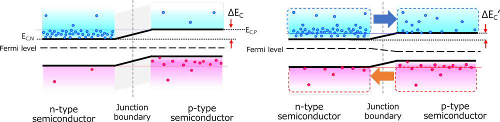
a) Unbiased
b) Forward bias
Fig. 2 : Energy band diagrams of a pn junction under zero bias and forward bias
Fig.2 shows the energy band diagram of a pn junction under no bias and forward bias conditions.
When a forward bias is applied, the effective barrier at the junction is reduced. As a result, the number of electrons that can cross the barrier from the n-type semiconductor into the p-type semiconductor increases. Consequently, the supply of electrons into the p-type region increases, and the minority carrier electron concentration at the junction edge, np(0), increases.
In the context of a BJT, this corresponds to the increase in the minority carrier electron concentration at the emitter side of the base region due to forward bias, i.e., the rise of the input boundary condition.
Supplement: Minority Carrier Concentration at the Junction Edge
Let np0 be the minority carrier electron concentration in the p-type region under no bias. When a forward bias VBE is applied, the electron concentration at the junction edge is given by:
np(0) = np0 exp(qVBE / kT)
2-2. Diffusion Transport in the Base and Collection at the B–C Junction (Output Condition: Low Concentration Maintained)
The injected electrons move through the base region by diffusion. In the active region, the B–C junction is reverse biased, creating a depletion region with an electric field directed toward the collector.
When electrons diffusing in the base reach the edge of the depletion region, they are immediately accelerated by the electric field and are efficiently swept into the collector (collection by drift).
Because electrons are continuously removed at the collector side, the electron concentration there remains low (fixed output condition). As a result, a concentration gradient from the emitter side (high) to the collector side (low) is maintained, and diffusion transport continues steadily under this gradient.
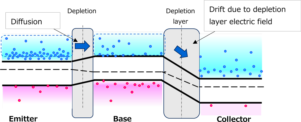
Fig. 3 : Energy band diagram of an NPN transistor in the active region
Fig.3 shows the energy band diagram of an NPN transistor in the active region.
Between the emitter and the base, carrier transport occurs by diffusion driven by the concentration gradient. Between the base and the collector, electrons are swept into the collector by the electric field in the depletion region (i.e., they are collected).
2-3. Carrier Loss in the Base and Asymmetry of Injection
- Loss by Recombination
Since the base is a p-type semiconductor containing majority carriers (holes), some of the injected electrons recombine with holes within the base region.
Although base current consists of several components, the dominant component corresponds to electrons lost due to recombination in the base. - Asymmetry of Injection
In an NPN BJT, the emitter is heavily doped n-type, while the base is lightly doped p-type.
Due to this asymmetry in doping, when the B–E junction is forward biased, electron injection from the emitter dominates, while hole injection from the base into the emitter is strongly suppressed. - Concentration Gradient in the Base
At the emitter side, np(0) is high, while at the collector side, electrons are rapidly removed by the depletion region electric field, keeping the concentration low.
Thus, a one-way concentration gradient is established across the base, driving diffusion current and enabling continuous carrier transport.
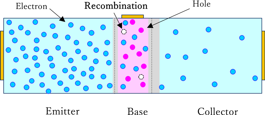
Fig. 4 : Carrier behavior in the base region in the active region (recombination and collection)
Fig.4 schematically illustrates the behavior of electron carriers in the base region in the active region (recombination and collection). A portion of the injected electrons recombines in the base and is lost, while the remainder is swept out at the B–C junction and collected by the collector.
2-4. Relation Between Base Current, Collector Current, and hFE
In the active region:
- Electron loss due to recombination corresponds to the base current IB
- Electrons that are collected correspond to the collector current IC
As long as the active-region operating conditions (input and output boundary conditions) are maintained, the fractions of carriers lost by recombination and collected by the collector do not change significantly. Therefore, when the injected carrier amount increases, both the recombination loss (IB) and the collected amount (IC) increase in proportion to the injected amount. This is the physical reason why IC increases proportionally with IB.
The proportionality is represented by the DC current gain hFE, defined as:
hFE = IC / IB
Thus, hFE does not arise from an additional "amplification mechanism," but is the observed result of carrier transport processes—"injection, recombination, and collection."
2-5. Summary of This Chapter (Active Region)
In the active region, the B–E junction is forward biased, increasing the input condition np(0), while the B–C junction is reverse biased, maintaining a low value at the output boundary condition. These input and output conditions establish a concentration gradient in the base. Electrons are transported by diffusion driven by this gradient and are efficiently collected by the depletion-region electric field.
Meanwhile, recombination loss occurs in the base, and this is observed as the base current IB. Because the loss fraction does not change significantly as long as the operating conditions are maintained, both IB and IC increase in proportion to the injected carrier amount, and hFE remains a valid current gain in the active region.
3. Why Current Amplification Does Not Hold in the Saturation Region (Breakdown of Internal Conditions)
In the saturation region, both the B–E and B–C junctions are forward biased.
This changes the boundary condition at the collector side: the electron concentration is no longer kept low and instead increases. As a result, the concentration gradient in the base becomes smaller.
Because the gradient is reduced, diffusion transport becomes less efficient. Electrons remain longer in the base, which increases recombination.
Consequently, the fraction of electrons reaching the collector decreases, and the collector current no longer increases proportionally with the base current.
3-1. Transition to the Saturation Region:
Change in Boundary Conditions (Output Condition)
The saturation region corresponds to a condition in which the base–emitter junction remains forward biased while the collector voltage VCE decreases, causing the base–collector junction to also become forward biased.
Under this condition, the requirement that the base–collector junction be reverse biased, which held in the active region, is no longer satisfied.
As a result, the electron concentration at the collector side of the base (i.e., the output boundary condition) is no longer fixed at a low value, and the conditions governing carrier transport are altered.
3-2. Change in Boundary Conditions and Resulting Modification of the Concentration Profile
(Reduction of the Concentration Gradient)
In the active region, the base–collector junction is reverse biased. Therefore, the electron concentration at the collector side is maintained at a low level, and a large concentration difference is established between the emitter side and the collector side. As a result, a well-defined electron concentration gradient is formed across the base from the emitter side toward the collector side. In contrast, in the saturation region, the base–collector junction is also forward biased, and the carrier transport condition differs from that in the active region even from the viewpoint of the energy band structure (see Figure 6).
In the active region, electrons are swept toward the collector by the electric field in the depletion region of the base–collector junction. In the saturation region, however, this electric field is weakened, and a small amount of electron supply (injection) from the collector into the base occurs. Although this injection is much smaller than the injection from the emitter, it raises the electron concentration at the collector side, reducing the concentration difference relative to the emitter side. Consequently, the concentration gradient formed in the base becomes more gradual, and the driving force for diffusion transport based on this gradient decreases.
In the active region, a large concentration gradient is established, enabling efficient diffusion transport. In the saturation region, however, the gradient is reduced, leading to a decrease in the efficiency of electron diffusion transport.
The resulting change in the concentration profile is shown in Figure 5. This change in carrier transport conditions can also be understood from the energy band structure (see Figure 6).
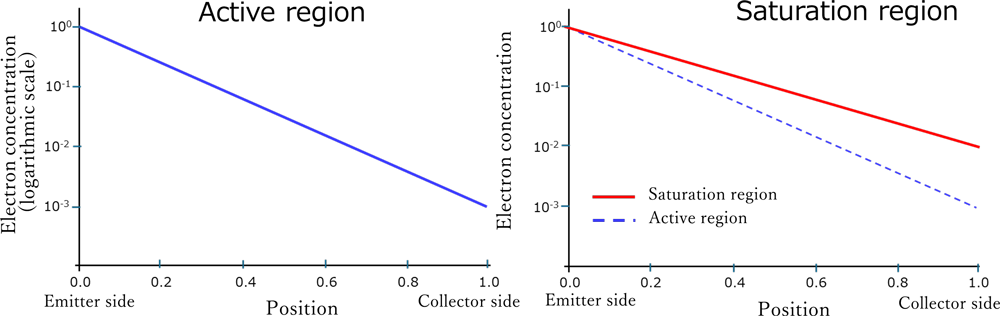
Fig. 5 : Electron concentration profiles in the base for active and saturation regions (log scale)
Fig.5 compares the electron concentration profiles in the base region (logarithmic scale) between the active region and the saturation region. In the active region, the electron concentration at the collector side is kept low, so a large concentration gradient (dn/dx) is formed in the base. In the saturation region, the electron concentration at the collector side increases, which reduces the concentration difference and makes the concentration gradient more gradual. The dashed line in the saturation-region plot indicates the active-region concentration profile for comparison. The vertical axis shows a relative value on a logarithmic scale, normalized such that the electron concentration at the emitter-side edge, np(0), is 1 (=10^0).
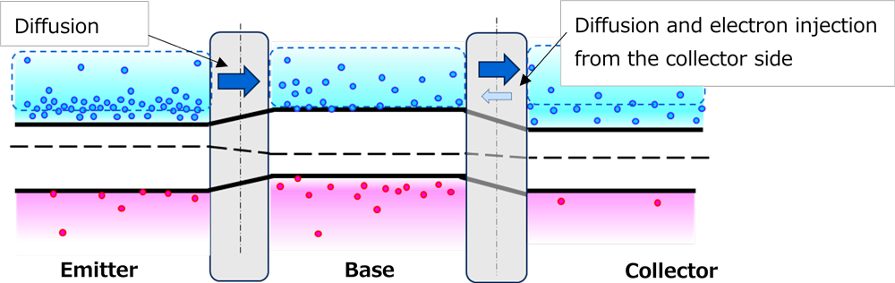
Fig. 6 : Energy band diagram of an NPN transistor in the saturation region
Fig.6 shows the energy band diagram of an NPN transistor in the saturation region. Diffusion transport between the emitter and the base remains dominant, as in the active region. In contrast, the base–collector junction becomes forward biased, which reduces the potential difference across the junction and weakens the electric field in the depletion region. As a result, electron transport between the base and the collector is also dominated by diffusion. In addition, a small amount of electron injection from the collector (where electrons are majority carriers) into the base occurs.
3-3. Increase in Carrier Residence Time and Recombination Due to Reduction of the Concentration Gradient
Even in the saturation region, as long as the base–emitter junction remains forward biased, electron injection from the emitter continues. However, as described in the previous section, the reduction of the concentration gradient leads to a decrease in the diffusion transport rate of electrons within the base region.
As a result, electron carriers remain in the base region for a longer time.
As the residence time increases, electrons stay longer in the base and are more likely to recombine with holes present in the base. Consequently, the fraction of electron carriers lost due to recombination increases. The fraction of electron carriers that can reach the collector therefore decreases, and even if the base current is increased, the collector current no longer increases proportionally as it does in the active region.
3-4. Behavior from a Circuit Perspective:
Loss of Meaning of hFE and Transition to Switch ON State
In the saturation region, increasing the base current no longer results in a proportional increase in the collector current. This behavior can also be understood from a circuit perspective.
In this region, the collector voltage decreases due to external circuit conditions, such as the load, and the operating point is determined under these voltage constraints. As a result, the collector current becomes primarily limited by the external circuit, rather than being controlled by the base current.
Therefore, although the ratio
hFE = IC / IB
can still be calculated, it no longer represents a meaningful measure of current control. This is because the collector current is no longer governed by the base current under these conditions.
For this reason, in the saturation region, the transistor does not function as a current amplification device, but instead operates as a switch in the ON state.
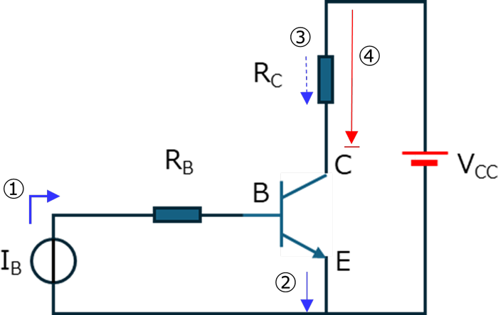
Fig. 7 : Common-emitter circuit in saturation and its relation to carrier transport
Fig.7 shows a common-emitter circuit operating in the saturation region and the corresponding internal carrier transport conditions. The sequence indicated by ① to ④ in the figure illustrates the following process.
As the base current IB increases, the emitter current IE increases accordingly. This leads to an increase in the collector current IC through the external load. However, the increased collector current causes a larger voltage drop across the load resistor, resulting in a decrease in the collector voltage VC (i.e., VCE).
As VCE decreases, the base–collector junction approaches forward bias, and the carrier transport conditions in the base region begin to change. Specifically, the concentration gradient of electrons is reduced, which increases the carrier residence time in the base and enhances recombination.
As a result, the collector current no longer increases proportionally with the base current, and the transistor enters the saturation region.
3-5. Summary of the Saturation Region
In the saturation region, forward biasing of the base–collector junction changes the output boundary condition and increases the electron concentration at the collector side, resulting in a reduction of the concentration gradient across the base.
As a result, the diffusion transport of electrons becomes less efficient, the carrier residence time in the base increases, and recombination losses become more significant.
Consequently, the collector current no longer increases proportionally with the base current, and the current gain hFE loses its meaning as an indicator of current control.
Under these conditions, the transistor no longer operates as a current amplification device, but instead functions as a switch in the ON state.
The term "saturation region" used for bipolar junction transistors (BJTs) has a significantly different physical meaning from that used for MOSFETs.
In BJTs, the saturation region refers to a condition in which current amplification no longer holds and the device operates as a switch. In contrast, in MOSFETs, the saturation region is one of the operating states in which a channel is formed, and it does not imply the breakdown of current amplification or switching behavior itself.
For a detailed explanation of MOSFET operating regions (cutoff, linear, and saturation) and their physical meaning, refer to the following FAQ:
Understanding MOSFET Operation Principles and Mechanisms | Cutoff, Linear, and Saturation Regions Explained
Related Links
The following documents also contain related information: