
- General Top
- SEMICONDUCTOR
- STORAGE
- COMPANY
-
My ToshibaSemicon
- Semiconductor Top
-
ApplicationsAutomotive
Body Electronics
xEV
In-Vehicle Infotainment
Advanced Driver-Assistance Systems (ADAS)
Chassis
IndustrialInfrastructure
BEMS/HEMS
Factory Automation
Commercial Equipment
Consumer/PersonalIoT Equipment
Healthcare
Wearable Device
Mobile
Computer Peripherals
-
ProductsAutomotive Devices
Discrete Semiconductor
Diodes
Transistors
Logic ICs
Analog Devices
- Automotive SmartMCD™ (Integreted SoC Conbining Microcontroller and Driver)
- Automotive Brushless Motor Driver ICs
- Automotive Brushed DC Motor Driver ICs
- Automotive Stepping Motor Driver ICs
- Automotive Driver ICs
- Automotive System Power Supplies ICs
- Automotive audio power amplifier ICs
- Automotive Network Communication
Digital Devices
Wireless Devices
※
 : Products list (parametric search)Power Semiconductors
SiC Power Devices
※
: Products list (parametric search)Isolators/Solid State RelaysPhotocouplers
Digital Isolators
Solid State Relays
Fiber Optic Transmitting Modules
※
: Products list (parametric search)MOSFETsIGBTs/IEGTsBipolar Transistors※
: Products list (parametric search)Diodes※
: Products list (parametric search)MicrocontrollersMotor Driver ICsIntelligent Power ICs※
: Products list (parametric search)Power Management ICsLinear ICs※
: Products list (parametric search)General Purpose Logic ICsLinear Image SensorsOther Product ICsOther Product ICs
※
: Products list (parametric search) -
Design & Development
-
Knowledge
- Where To Buy


- Part Number & Keyword Search
- Cross Reference Search
- Parametric Search
- Stock Check & Purchase
This webpage doesn't work with Internet Explorer. Please use the latest version of Google Chrome, Microsoft Edge, Mozilla Firefox or Safari.
require 3 characters or more. Search for multiple part numbers fromhere.
The information presented in this cross reference is based on TOSHIBA's selection criteria and should be treated as a suggestion only. Please carefully review the latest versions of all relevant information on the TOSHIBA products, including without limitation data sheets and validate all operating parameters of the TOSHIBA products to ensure that the suggested TOSHIBA products are truly compatible with your design and application.Please note that this cross reference is based on TOSHIBA's estimate of compatibility with other manufacturers' products, based on other manufacturers' published data, at the time the data was collected.TOSHIBA is not responsible for any incorrect or incomplete information. Information is subject to change at any time without notice.
require 3 characters or more.
Automotive MOSFETs with Small Package Featuring Wettable Flank Structure
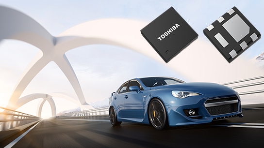
Toshiba Electronic Devices & Storage Corporation ("Toshiba") has launched five products of automotive MOSFETs that combine space-saving and high-mountability by using small DFN2020B(WF) package with a wettable flank structure[1]. The N-channel MOSFETs are "XSM6K361NW, XSM6K519NW, XSM6K376NW, and XSM6K336NW," and the P-channel MOSFET is "XSM6J372NW."
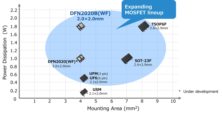
The DFN2020B(WF) package adopts a wettable flank structure, which improves solder wettability compared to Toshiba’s existing UDFN6B package. In addition, the improved visibility of the solder fillet[2] allows for confirmation of solderability in automatic visual inspection (AVI) equipment, contributing to the automation of inspection on the manufacturing line. Furthermore, in the solder joint mounting shear strength[3] test, it is approximately 23%[4] stronger than Toshiba’s existing SOT-23F[5] package, contributing to improved reliability of the equipment.
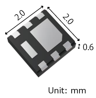
The package size of DFN2020B(WF) is 2.0×2.0×0.6mm (typ.), which reduces the mounting area by approximately 43% and the package height by approximately 25% compared to the SOT-23F package, contributing to the miniaturization of equipment. Furthermore, it features a high power dissipation despite a small package. The maximum power dissipation rating of XSM6K361NW, one of new products, is 1.84W[6].
The new products comply with AEC-Q101, the automotive industry standard reliability test specification. The PPAP[7] of IATF16949, the international standard for quality management systems specific to the automotive industry, is available[8]. These products can be used in various automotive applications such as DC-DC converters in ECUs[9] and LED headlamp load switches.
Toshiba will continue to expand its lineup of MOSFET and 2in1 MOSFET products for automotive applications, housed in packages with wettable flank structure.
Notes:
[1] Shape of side leads of package.
[2] Solder fillet refers to the soldered portion of a component mounted on a printed circuit board.
[3] Mounting shear strength is one of the testing methods for evaluating the strength of joints in electronic components and semiconductor packages.
[4] Toshiba compared with mean of actual measured value.
[5] Existing products such as SSM3K361R, the package size: 2.4×2.9×0.8mm (typ.)
[6] Device mounted on a 25.4×25.4×1.6mm, Cu pad: 645mm2, FR-4 glass epoxy board
[7] PPAP: Abbreviation for Production Part Approval Process, a mass-produced part approval processing.
[8] Please contact Toshiba sales representatives for more details
[9] ECU: Abbreviation for Electronic Control Unit, an electronic device for controlling various functions of a vehicle.
Features
- Package with wettable flank structure enables automatic visual inspection of board mounting conditions
- Small, low profile high power dissipation package
Features Explanation
1. Package with wettable flank structure enables automatic visual inspection of board mounting conditions
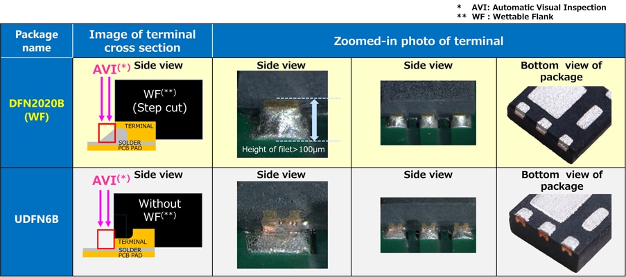
By adopting a wettable flank structure, the solder fillet visibility is improved compared to Toshiba’s existing UDFN6B package. This allows for solder joint inspection using automatic visual inspection (AVI) equipment, contributing to the automation of inspections on the production line.
2. Small, low profile high power dissipation package
DFN2020B(WF) packages have higher power dissipation than SOT-23F packages. The maximum power dissipation rating of XSM6K361NW, one of new products, is 1.84W[6], approximately 1.5 times higher than 1.2W[6] of Toshiba’s existing product SSM3K361R with SOT-23F package. Therefore, the new products contribute to the development of various automotive equipment such as DC-DC converters for ECUs that require compact size and high power dissipation MOSFETs and load switches for LED headlamps.
Applications
Automotive equipment
- DC-DC converters for ECUs, load switches for LED headlamps, etc.
Main Specifications
(Ta=25°C)
| Part number | XSM6K361NW | XSM6K519NW | XSM6K376NW | XSM6K336NW | XSM6J372NW | |||
|---|---|---|---|---|---|---|---|---|
| Polarity | N-channel | P-channel | ||||||
| Package | Name | DFN2020B(WF) | ||||||
| Size (mm) | Typ. | 2.0×2.0×0.6 | ||||||
| Absolute maximum ratings | Drain-source voltage VDSS (V) |
100 | 40 | 30 | 30 | -30 | ||
| Gate-source voltage VGSS (V) |
+20/-20 | +20/-20 | +12/-8 | +20/-20 | -12/+6 | |||
| Drain current (DC) ID (A) |
3.5 | 8.0 | 4.0 | 3.0 | -6.0 | |||
| Power dissipation PD[6] (W) |
1.84 | 1.84 | 1.53 | 1.53 | 1.53 | |||
| Electrical character istics |
Drain-source On-resistance RDS(ON) (mΩ) |
VGS=|10V| | Max | 69 | 17.8 | - | 95 | 42 |
| VGS=|4.5V| | Max | 92 | 36.3 | 56 | 140 | 50 | ||
| VGS=|2.5V| | Max | - | - | 72 | - | 72 | ||
| VGS=|1.8V| | Max | - | - | 109 | - | 144 | ||
| Input capacitance Ciss (pF) | Typ. | 430 | 797 | 200 | 126 | 560 | ||
| Total gate charge Qg (nC) | Typ. | 3.2 | 6.5 | 2.2 | 1.7 | 8.2 | ||
| Sample Check & Availability |  |
|
|
|
|
|||
Related Contents
Refer to the following page for details on new products.
XSM6K361NW
XSM6K519NW
XSM6K376NW
XSM6K336NW
XSM6J372NW
DFN2020B(WF) videos of the package are shown in the link below.
DFN2020B(WF) package
Follow the link below for more on Toshiba Automotive MOSFETs.
Automotive MOSFETs
For examples of applications, see the following pages.
Automotive LED Headlamp
IVI (In-vehicle Infotainment)
Stock Check & Purchase
require 3 characters or more.
Through this website you are able to proceed to the website of our distributors ("Third Party Website") which is not under the control of Toshiba Corporation and its subsidiaries and affiliates (collectively "Toshiba"). The Third Party Website is made available to you as a convenience only and you agree to use the Third Party Website at your own risk. The link of the Third Party Website does not necessarily imply a recommendation or an endorsement by Toshiba of the Third Party Website. Please be aware that Toshiba is not responsible for any transaction done through the Third Party Website, and such transactions shall be subject to terms and conditions which may be provided in the Third Party Website.
* Company names, product names, and service names may be trademarks of their respective companies.
* Information in this document, including product prices and specifications, content of services and contact information, is current on the date of the announcement but is subject to change without prior notice.