- General Top
- SEMICONDUCTOR
- STORAGE
- COMPANY
-
My ToshibaSemicon
- Semiconductor Top
-
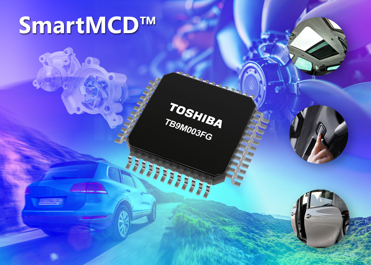
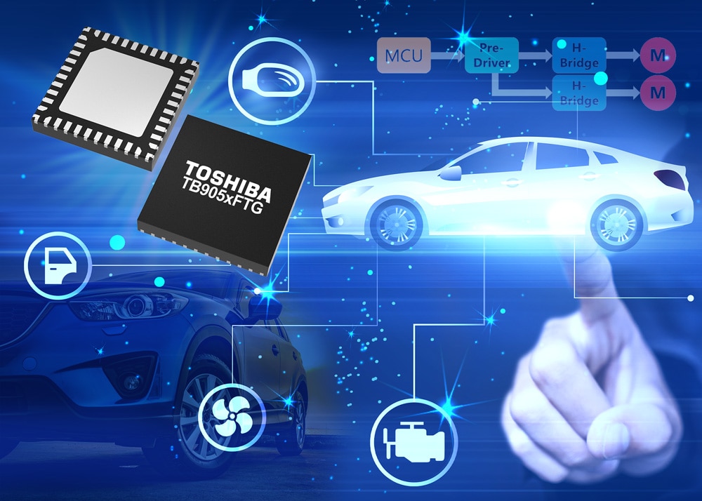
ApplicationsAutomotive
Body Electronics
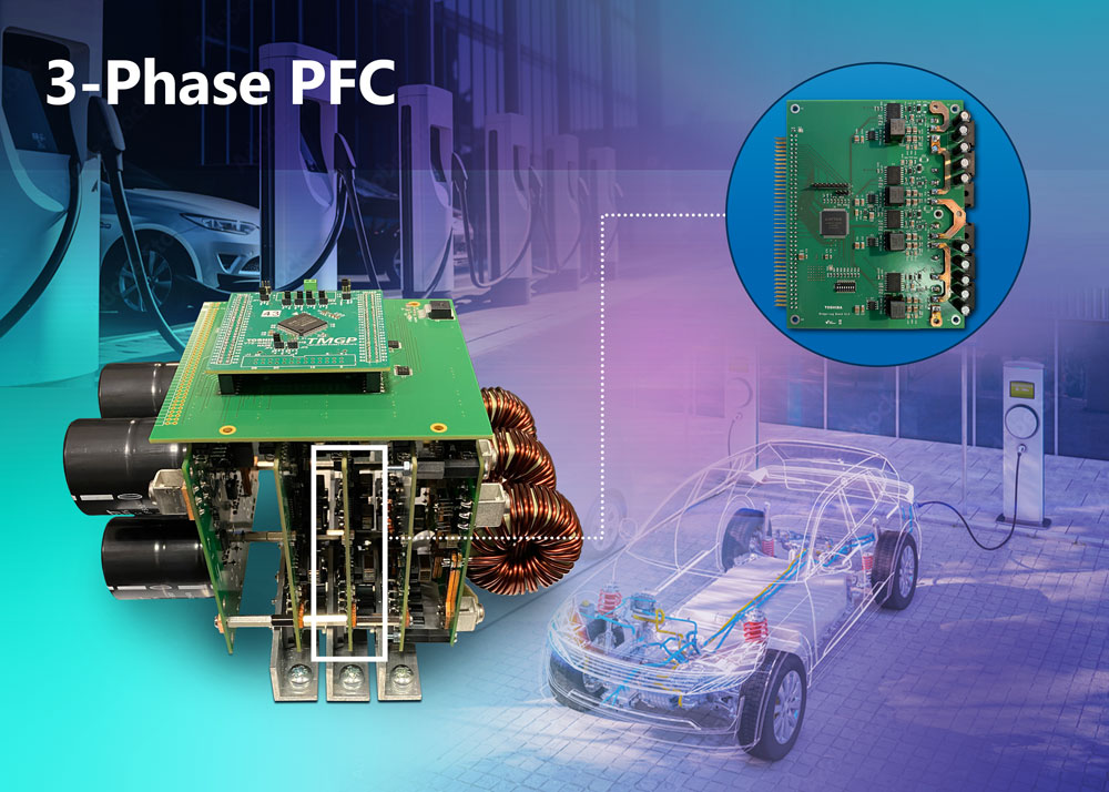
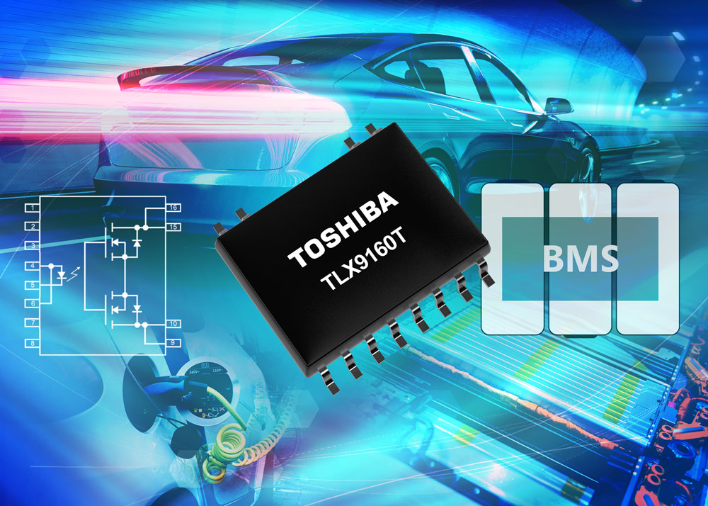
xEV
In-Vehicle Infotainment
Advanced Driver-Assistance Systems (ADAS)
Chassis
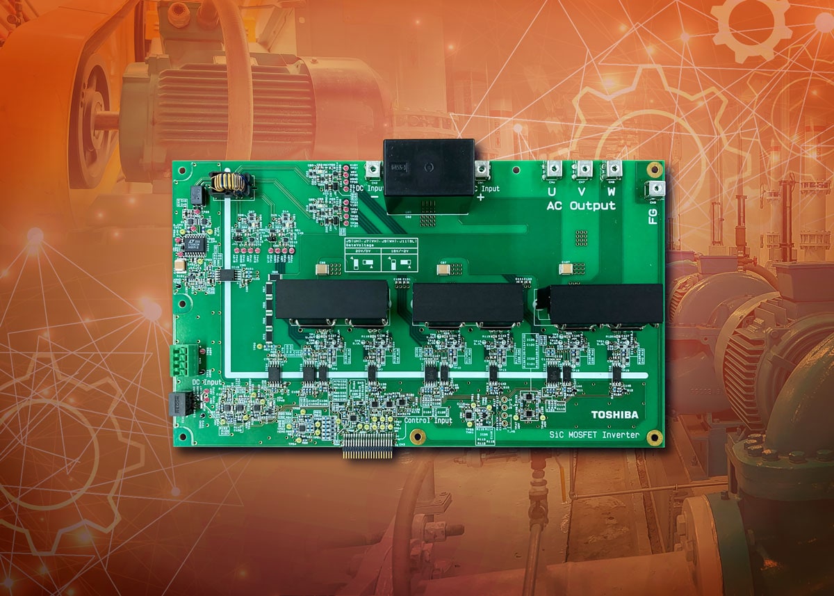
IndustrialInfrastructure
BEMS/HEMS
Factory Automation
Commercial Equipment
Consumer/PersonalIoT Equipment
Healthcare
Wearable Device
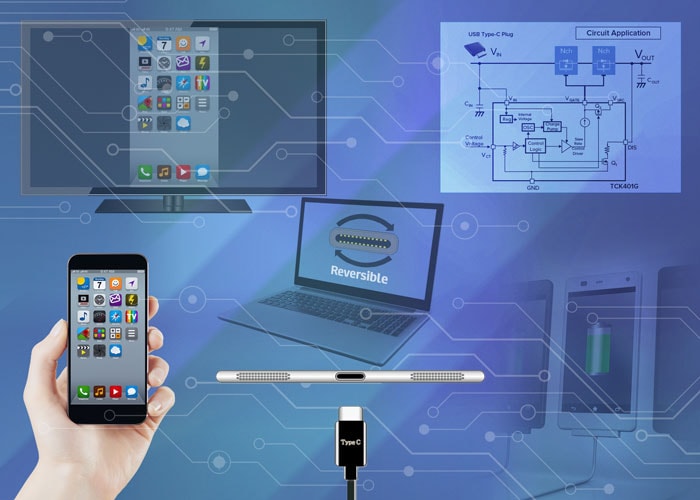
Mobile
Computer Peripherals
-
ProductsAutomotive Devices
Discrete Semiconductor
Diodes
Transistors
Logic ICs
Analog Devices
Digital Devices
Wireless Devices
※
 : Products list (parametric search)Power Semiconductors
SiC Power Devices
※
: Products list (parametric search)Isolators/Solid State RelaysPhotocouplers
Digital Isolators
Solid State Relays
Fiber Optic Transmitting Modules
※
: Products list (parametric search)MOSFETsIGBTs/IEGTsBipolar Transistors※
: Products list (parametric search)Diodes※
: Products list (parametric search)MicrocontrollersMotor Driver ICsIntelligent Power ICs※
: Products list (parametric search)Power Management ICsLinear ICs※
: Products list (parametric search)General Purpose Logic ICsLinear Image SensorsOther Product ICsOther Product ICs
※
: Products list (parametric search) -
Design & Development
Design & Development
Innovation Centre
At the Toshiba Innovation Centre we constantly strive to inspire you with our technologies and solutions. Discover how to place us at the heart of your innovations.
-
Knowledge
Knowledge
Highlighted Topics
Further Materials
Other
- Where To Buy


- Part Number & Keyword Search
- Cross Reference Search
- Parametric Search
- Stock Check & Purchase
This webpage doesn't work with Internet Explorer. Please use the latest version of Google Chrome, Microsoft Edge, Mozilla Firefox or Safari.
require 3 characters or more. Search for multiple part numbers fromhere.
The information presented in this cross reference is based on TOSHIBA's selection criteria and should be treated as a suggestion only. Please carefully review the latest versions of all relevant information on the TOSHIBA products, including without limitation data sheets and validate all operating parameters of the TOSHIBA products to ensure that the suggested TOSHIBA products are truly compatible with your design and application.Please note that this cross reference is based on TOSHIBA's estimate of compatibility with other manufacturers' products, based on other manufacturers' published data, at the time the data was collected.TOSHIBA is not responsible for any incorrect or incomplete information. Information is subject to change at any time without notice.
require 3 characters or more.
Incremental improvements deliver significant benefits to high-power automotive applications
Modern vehicles are employing more electronics than ever before to make them more efficient and ultimately, safer. Improved efficiency not only reduces vehicle running costs but also means less heat is generated in the on-board electronic systems. This, in turn, means those systems can operate with less cooling, allowing them to become smaller. Smaller systems are, by definition, lighter - which also has a positive impact on the efficiency of the vehicle.
Consumers see the benefit of enhanced in-vehicle technology in terms of greater functionality in areas such as comfort, infotainment, security, connectivity and driver assistance systems. The increased efficiency has a particular impact on EVs and HEVs that will travel further on a single charge.
Yet, seemingly simple changes and small improvements in semiconductor components are behind these efficiency improvements.
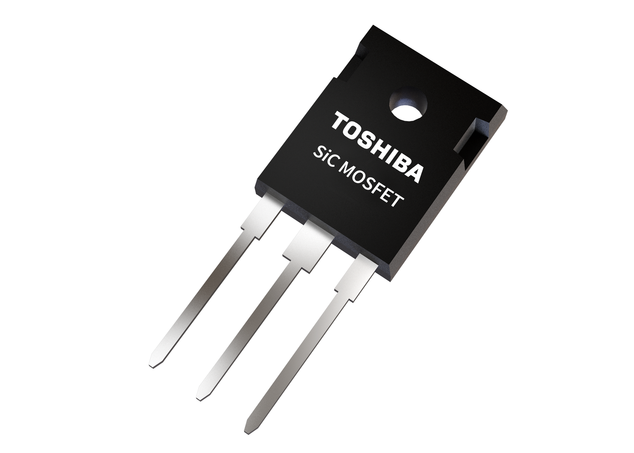
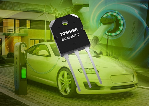
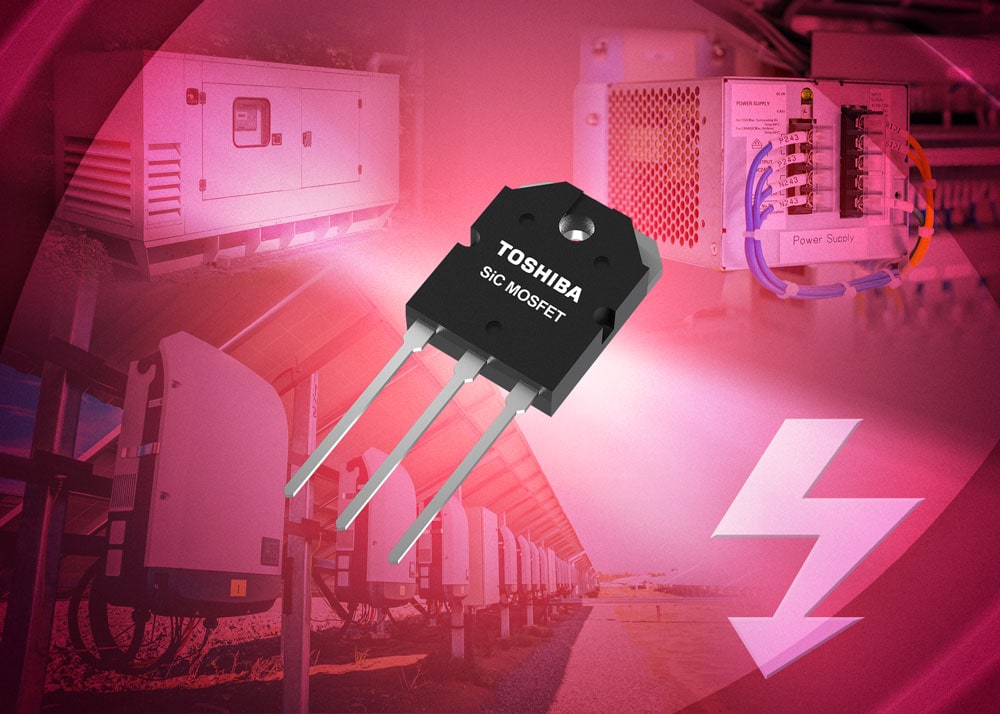
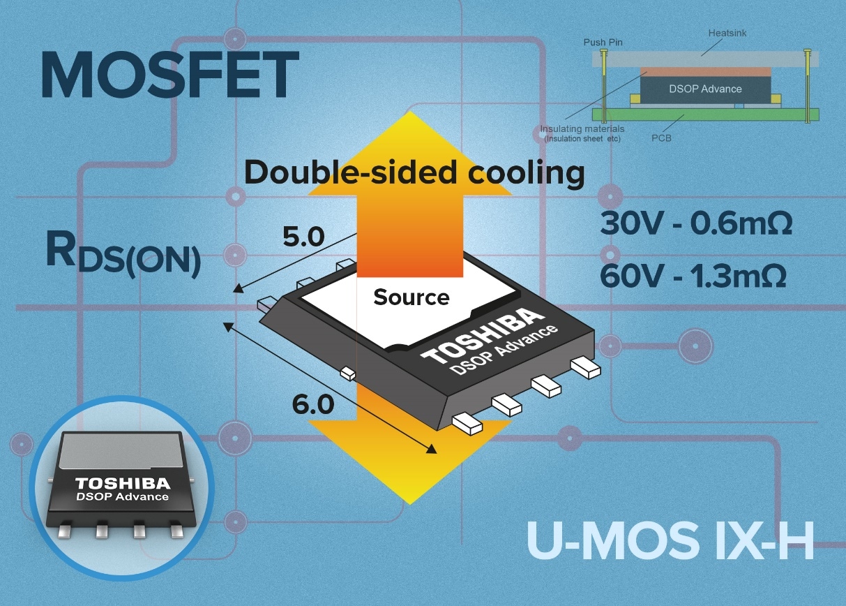
Some of the most important components in modern vehicles are the MOSFETs that switch the power needed for pumps and fans to turn, seats to move or locks to operate.
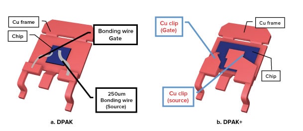
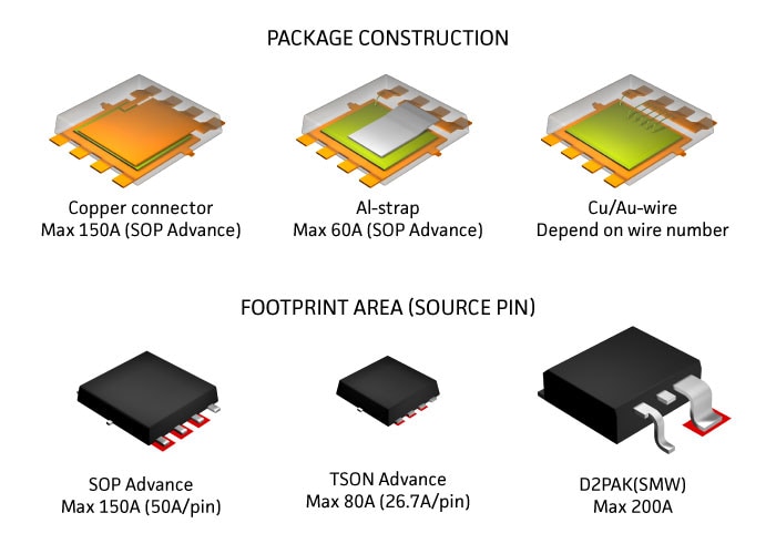
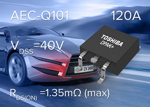
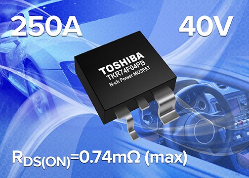
Toshiba has developed a novel copper connector technology for key MOSFETs that are used in automotive applications. This is used in the unique TO-220SM(W) SMD power package that measures 10mm x 13mm and incorporates a 3x wider and shorter source pin than a conventional D2PAK package.
Due to the improved source pin dimensions, package resistance is reduced by about 0.15mΩ. Compare, for example, Toshiba’s TK1R4F04PB 40V, 1.35mΩ (max) MOSFET in the TO-220SM(W) package with the TK1R5R04PB 40V, 1.5mΩ (max) MOSFET in D2PAK+. While both use the same chip within the package, the on-resistance (RDS(ON)) of TK1R4F04PB is 0.15mΩ lower than that of the TK1R5R04PB.
These extremely low values would simply not be possible without the combination of Toshiba’s established copper connecter technology, its unique TO-220SW(W) package technology, and a highly advanced wafer process.
In automotive applications where currents can be very large (and potential losses, therefore, significant) improvements of just 0.15mΩ in RDS(ON are very significant.
A comprehensive white paper describing how the latest high-performance MOSFETs are enabling automotive power systems has been published by Toshiba. For more information visit