
- General Top
- SEMICONDUCTOR
- STORAGE
- COMPANY
-
My ToshibaSemicon
- Semiconductor Top
-
ApplicationsAutomotive
Body Electronics
xEV
In-Vehicle Infotainment
Advanced Driver-Assistance Systems (ADAS)
Chassis
IndustrialInfrastructure
BEMS/HEMS
Factory Automation
Commercial Equipment
Consumer/PersonalIoT Equipment
Healthcare
Wearable Device
Mobile
Computer Peripherals
-
ProductsAutomotive Devices
Discrete Semiconductor
Diodes
Transistors
Logic ICs
Analog Devices
- Automotive SmartMCD™ (Integreted SoC Conbining Microcontroller and Driver)
- Automotive Brushless Motor Driver ICs
- Automotive Brushed DC Motor Driver ICs
- Automotive Stepping Motor Driver ICs
- Automotive Driver ICs
- Automotive System Power Supplies ICs
- Automotive audio power amplifier ICs
- Automotive Network Communication
Digital Devices
Wireless Devices
※
 : Products list (parametric search)Power Semiconductors
SiC Power Devices
※
: Products list (parametric search)Isolators/Solid State RelaysPhotocouplers
Digital Isolators
Solid State Relays
Fiber Optic Transmitting Modules
※
: Products list (parametric search)MOSFETsIGBTs/IEGTsBipolar Transistors※
: Products list (parametric search)Diodes※
: Products list (parametric search)MicrocontrollersMotor Driver ICsIntelligent Power ICs※
: Products list (parametric search)Power Management ICsLinear ICs※
: Products list (parametric search)General Purpose Logic ICsLinear Image SensorsOther Product ICsOther Product ICs
※
: Products list (parametric search) -
Design & Development
-
Knowledge
- Where To Buy


- Part Number & Keyword Search
- Cross Reference Search
- Parametric Search
- Stock Check & Purchase
This webpage doesn't work with Internet Explorer. Please use the latest version of Google Chrome, Microsoft Edge, Mozilla Firefox or Safari.
require 3 characters or more. Search for multiple part numbers fromhere.
The information presented in this cross reference is based on TOSHIBA's selection criteria and should be treated as a suggestion only. Please carefully review the latest versions of all relevant information on the TOSHIBA products, including without limitation data sheets and validate all operating parameters of the TOSHIBA products to ensure that the suggested TOSHIBA products are truly compatible with your design and application.Please note that this cross reference is based on TOSHIBA's estimate of compatibility with other manufacturers' products, based on other manufacturers' published data, at the time the data was collected.TOSHIBA is not responsible for any incorrect or incomplete information. Information is subject to change at any time without notice.
require 3 characters or more.
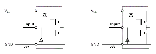
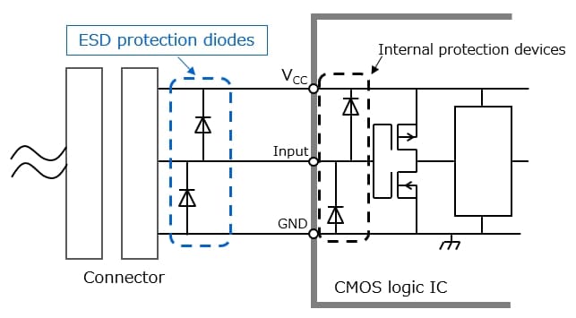
1-1. Handling of Unused Input Pins
Generally, all unused inputs should be tied to either VCC or GND.
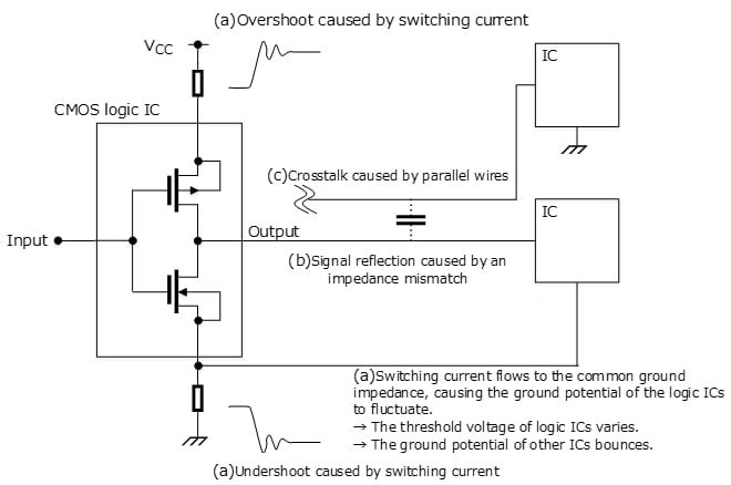
However, any pins of bidirectional bus buffers (e.g., Function 245) that can be configured as an output (e.g., bus pins) should be tied to VCC via a pull-up resistor or to GND via a pull-down resistor. It is recommended that both ends of the buffer be pulled up or down to the same potential to avoid unnecessary current flow. However, leave the input pins with bushold, such as those of the ICs of the TC74VCXHxxx Series, open. Large inrush current due to parasitic capacitance (in the order of a few milliamperes) can be a problem even with typical CMOS logic ICs when their power supply is on. In order to improve system reliability against device destruction and other failures, their inputs can be tied to VCC via a pull-up resistor or to GND via a pull-down resistor.
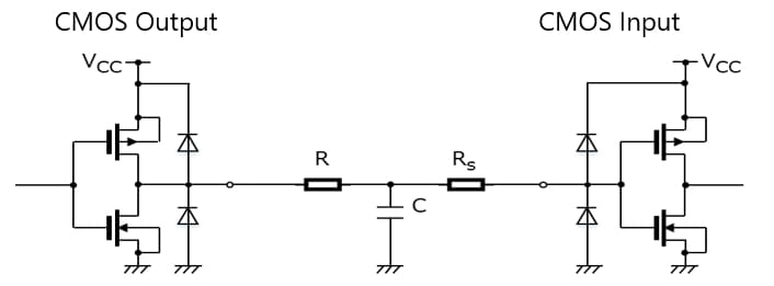
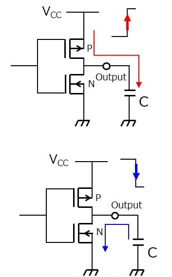
Because CMOS logic has a very high input impedance, any open input might result in a false output value due to the influence of a surrounding electric field. In addition, shoot-through current might flow at the midpoint of VCC and GND, causing an increase in supply current and leading to device destruction in the worst-case scenario.
Be sure to apply these considerations to all inputs without a bushold capability unless otherwise instructed in the datasheet.

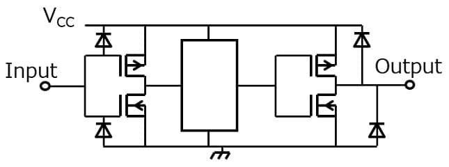
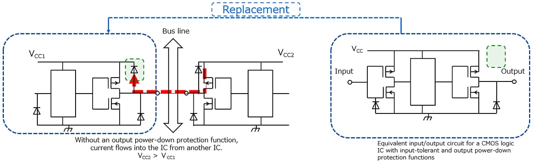
Usage Considerations of CMOS Logic ICs


Products
Related information
- Application Notes
- FAQ