
- General Top
- SEMICONDUCTOR
- STORAGE
- COMPANY
-
My ToshibaSemicon
- Semiconductor Top
-
ApplicationsAutomotive
Body Electronics
xEV
In-Vehicle Infotainment
Advanced Driver-Assistance Systems (ADAS)
Chassis
IndustrialInfrastructure
BEMS/HEMS
Factory Automation
Commercial Equipment
Consumer/PersonalIoT Equipment
Healthcare
Wearable Device
Mobile
Computer Peripherals
-
ProductsAutomotive Devices
Discrete Semiconductor
Diodes
Transistors
Logic ICs
Analog Devices
- Automotive SmartMCD™ (Integreted SoC Conbining Microcontroller and Driver)
- Automotive Brushless Motor Driver ICs
- Automotive Brushed DC Motor Driver ICs
- Automotive Stepping Motor Driver ICs
- Automotive Driver ICs
- Automotive System Power Supplies ICs
- Automotive audio power amplifier ICs
- Automotive Network Communication
Digital Devices
Wireless Devices
※
 : Products list (parametric search)Power Semiconductors
SiC Power Devices
※
: Products list (parametric search)Isolators/Solid State RelaysPhotocouplers
Digital Isolators
Solid State Relays
Fiber Optic Transmitting Modules
※
: Products list (parametric search)MOSFETsIGBTs/IEGTsBipolar Transistors※
: Products list (parametric search)Diodes※
: Products list (parametric search)MicrocontrollersMotor Driver ICsIntelligent Power ICs※
: Products list (parametric search)Power Management ICsLinear ICs※
: Products list (parametric search)General Purpose Logic ICsLinear Image SensorsOther Product ICsOther Product ICs
※
: Products list (parametric search) -
Design & Development
-
Knowledge
- Where To Buy


- Part Number & Keyword Search
- Cross Reference Search
- Parametric Search
- Stock Check & Purchase
This webpage doesn't work with Internet Explorer. Please use the latest version of Google Chrome, Microsoft Edge, Mozilla Firefox or Safari.
require 3 characters or more. Search for multiple part numbers fromhere.
The information presented in this cross reference is based on TOSHIBA's selection criteria and should be treated as a suggestion only. Please carefully review the latest versions of all relevant information on the TOSHIBA products, including without limitation data sheets and validate all operating parameters of the TOSHIBA products to ensure that the suggested TOSHIBA products are truly compatible with your design and application.Please note that this cross reference is based on TOSHIBA's estimate of compatibility with other manufacturers' products, based on other manufacturers' published data, at the time the data was collected.TOSHIBA is not responsible for any incorrect or incomplete information. Information is subject to change at any time without notice.
require 3 characters or more.
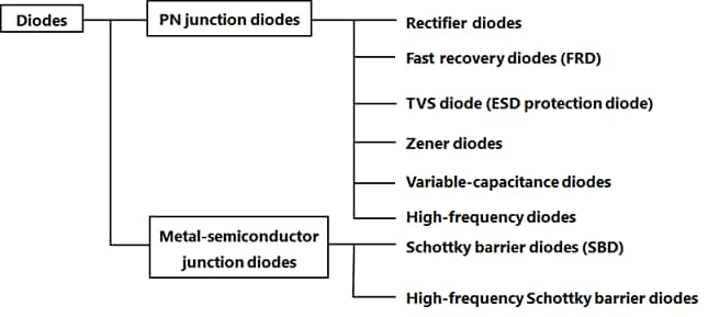
2-10. Schottky Barrier Diodes (SBDs)
Download "Chapter II : Diodes" (PDF:895KB)
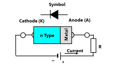
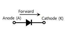
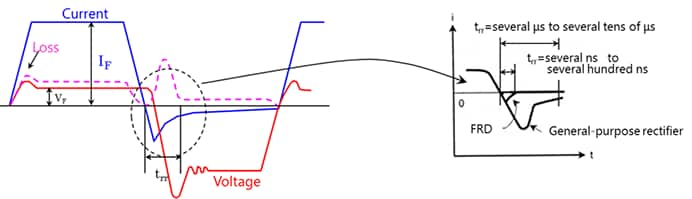
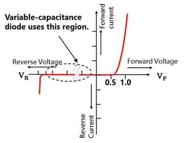
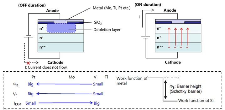
A Schottky barrier diode (SBD) is a device in which a semiconductor and a metal such as molybdenum are bonded instead of a pn junction. In general, SBDs of n-type semiconductor and metal junctions are commercialized. It is suitable for high-speed switching applications, because of small forward voltage and short reverse recovery time[Note].
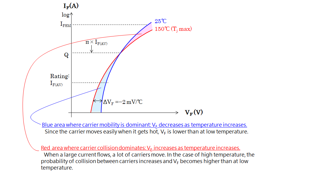
For the SBD there is a tradeoff between forward voltage (VF) and reverse current.
Depending on the metal used, in general, the breakdown voltage is about 20 to 150 V and the VF is about 0.4 to 0.7 V, which is lower than that of the pn junction diode.
SBDs with a new structure with low forward voltage but low reverse current have also been commercialized.
(Toshiba has achieved low VF and low reverse current characteristics by adopting a trench structure for SBD. )
Note: Since SBD is a unipolar device, it does not have reverse recovery time due to carrier recombination like pn junction diodes. However, the current waveform charging the capacity between the terminals of SBD is observed like the reverse recovery time of the p-n junction diode.
Therefore, it is described as reverse recovery time in this document.

Chapter II : Diodes


Related information
- Products
- FAQ