
- General Top
- SEMICONDUCTOR
- STORAGE
- COMPANY
-
My ToshibaSemicon
- Semiconductor Top
-
ApplicationsAutomotive
Body Electronics
xEV
In-Vehicle Infotainment
Advanced Driver-Assistance Systems (ADAS)
Chassis
IndustrialInfrastructure
BEMS/HEMS
Factory Automation
Commercial Equipment
Consumer/PersonalIoT Equipment
Healthcare
Wearable Device
Mobile
Computer Peripherals
-
ProductsAutomotive Devices
Discrete Semiconductor
Diodes
Transistors
Logic ICs
Analog Devices
- Automotive SmartMCD™ (Integreted SoC Conbining Microcontroller and Driver)
- Automotive Brushless Motor Driver ICs
- Automotive Brushed DC Motor Driver ICs
- Automotive Stepping Motor Driver ICs
- Automotive Driver ICs
- Automotive System Power Supplies ICs
- Automotive audio power amplifier ICs
- Automotive Network Communication
Digital Devices
Wireless Devices
※
 : Products list (parametric search)Power Semiconductors
SiC Power Devices
※
: Products list (parametric search)Isolators/Solid State RelaysPhotocouplers
Digital Isolators
Solid State Relays
Fiber Optic Transmitting Modules
※
: Products list (parametric search)MOSFETsIGBTs/IEGTsBipolar Transistors※
: Products list (parametric search)Diodes※
: Products list (parametric search)MicrocontrollersMotor Driver ICsIntelligent Power ICs※
: Products list (parametric search)Power Management ICsLinear ICs※
: Products list (parametric search)General Purpose Logic ICsLinear Image SensorsOther Product ICsOther Product ICs
※
: Products list (parametric search) -
Design & Development
-
Knowledge
- Where To Buy


- Part Number & Keyword Search
- Cross Reference Search
- Parametric Search
- Stock Check & Purchase
This webpage doesn't work with Internet Explorer. Please use the latest version of Google Chrome, Microsoft Edge, Mozilla Firefox or Safari.
require 3 characters or more. Search for multiple part numbers fromhere.
The information presented in this cross reference is based on TOSHIBA's selection criteria and should be treated as a suggestion only. Please carefully review the latest versions of all relevant information on the TOSHIBA products, including without limitation data sheets and validate all operating parameters of the TOSHIBA products to ensure that the suggested TOSHIBA products are truly compatible with your design and application.Please note that this cross reference is based on TOSHIBA's estimate of compatibility with other manufacturers' products, based on other manufacturers' published data, at the time the data was collected.TOSHIBA is not responsible for any incorrect or incomplete information. Information is subject to change at any time without notice.
require 3 characters or more.
Small-Package Photorelays for Semiconductor Testers Combining High ON-State Current and Low OFF-State Leakage Current
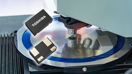
Toshiba Electronic Devices & Storage Corporation (“Toshiba”) has launched two photorelays, "TLP3487" and "TLP3491", for semiconductor testers, featuring small P‑SON4 [1] packages that achieve both high ON‑state current and low OFF‑state leakage current.
A semiconductor tester (ATE: Automatic Test Equipment) is a system that applies voltages and currents to each pin of a device under test (DUT), such as system LSIs and semiconductor memories, to verify proper operation. In such testers, it is necessary to switch power and signal paths for each pin of the DUT; therefore, photorelays—a type of solid‑state relay with MOSFET outputs—are widely used. On the other hand, in semiconductor testers, OFF‑state leakage current of relays can cause measurement errors, making the reduction of leakage current essential for improving measurement accuracy. In addition, applications such as power supply and load control also require support for high current, creating a need for switching devices that can satisfy these requirements at a high level.
The new products TLP3487 and TLP3491 achieve both high ON‑state current and low OFF‑state leakage current through optimized device design of the MOSFET output section—performance that was difficult to realize with Toshiba’s existing P‑SON4 package photorelays[2]. Previously, in applications requiring high current, multiple devices have often been used in combination. As a result, this has led to issues such as an increased mounting area due to a higher component count and increased OFF‑state leakage current. Since TLP3487 and TLP3491 support both high ON‑state current and low OFF‑state leakage current, they can be configured as a single device, contributing to a reduction in component count and board space.
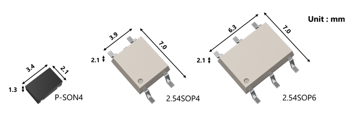
In addition, by adopting the P‑SON4 package, the mounting area can be reduced by approximately 74% compared with the 2.54SOP4 package and by approximately 84% compared with the 2.54SOP6 package used in Toshiba’s existing products, supporting high‑density mounting.
With these features, the new products are suitable for high‑precision measurement applications requiring low OFF‑state leakage current, and can be used in a wide range of semiconductor tester applications, including memory testers and SoC testers.
Toshiba will continue to pursue further reductions in OFF‑state leakage current, support for higher current, and miniaturization of photorelays, expanding its product lineup to meet the needs for higher precision and higher density in semiconductor testers.
Notes:
[1] P‑SON4: Power Small Outline Non‑leaded
[2] Toshiba’s existing product TLP3481, etc.
Features
- Low OFF‑state current (IOFF) characteristics that minimize the impact on measurement signals
- Capable of use in locations where large currents flow, with an ON‑state current (ION) of 2A (max)
- Small P‑SON4 package suitable for high‑density mounting
Features Explanation
1. Low OFF‑state current (IOFF) characteristics that minimize the impact on measurement signals
In tester applications, even a small amount of current flowing when the relay is in the off state (leakage) can cause errors in measurement values and signals. Therefore, minimizing OFF‑state current (IOFF) is essential for improving measurement accuracy. The new products optimize the device design of the MOSFET output stage to simultaneously achieve both high ON‑state current and low OFF‑state leakage current—an approach that was difficult to realize with small packages—and, compared with existing products[3], can suppress leakage current when the relay is off.
- TLP3487: OFF‑state current (IOFF) of 10nA (VOFF=60V) (max)
- TLP3491: OFF‑state current (IOFF) of 1nA (VOFF=40V) (max)
Note:
[3] TLP3481 (OFF‑state current (IOFF) of 10nA (max) at VOFF=40V, and 1μA (max) at VOFF=60V)
2.Capable of use in locations where large currents flow, with an ON‑state current (ION) of 2A (max)
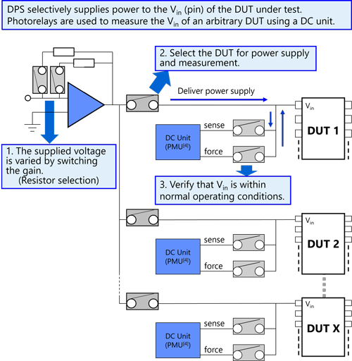
In semiconductor testers, not only signal switching but also paths for supplying power to the DUT—such as device power supplies (DPS)—handle high currents on the order of several amperes. Therefore, switching devices are also required to have high current capability.
Since both new products support an ON‑state current (ION) of 2A (max), they can be used in applications where large currents flow, including power supply and load control.
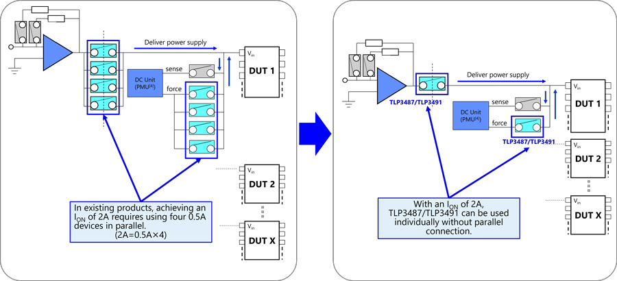
Conventionally, in applications requiring high current, multiple devices have often been used in combination. However, such configurations can lead to issues such as an increase in mounting area due to a higher component count and the possibility of increased OFF‑state leakage current resulting from the combined configuration.
Because the TLP3487 and TLP3491 simultaneously achieve both high ON‑state current and low OFF‑state leakage current, they can be readily configured using a single device, contributing to a reduction in component count and board space (Figure 2).
Note:
[4] PMU stands for Parametric Measurement Unit. It is a DC measurement unit that applies voltage or current to the DUT (Device Under Test) and measures the resulting current or voltage as a response.
3.Small P‑SON4 package suitable for high‑density mounting
In semiconductor testers, multiple DUTs are measured simultaneously, requiring a large number of relays to be mounted on a limited test board area. While technological innovations such as higher processing speeds continue to advance, there is also increasing demand for cost reduction and high reliability, making higher test board density unavoidable.
By adopting the P‑SON4 package, the new product features a compact mounting area of 7.2mm2 (typ.). This enables a reduction in mounting area of approximately 74% compared with the conventional 2.54SOP4 package and approximately 84% compared with the 2.54SOP6 package, thereby supporting high‑density mounting.
Applications
- Semiconductor testers used to evaluate memories, SoC, LSI, etc.
- Peripheral equipment for semiconductor testers (probe cards, test interface boards [load boards], I/O interface boards, etc.)
Main Specifications
(Unless otherwise specified, Ta=25℃)
| Part number | TLP3487 | TLP3491 | |||
|---|---|---|---|---|---|
| Contact | 1a (Normally opened) |
||||
| Package | Name | P-SON4 | |||
| Size (mm) | Typ. | 3.4×2.1×1.3 | |||
| Absolute maximum ratings |
OFF-state output terminal voltage VOFF (V) | 60 | |||
| ON-state current ION (A) | 2 | ||||
| ON-state current (pulsed) IONP (A) | 6 | ||||
| Operating temperature Topr (°C) | -40 to 110 | ||||
| Coupled electrical characteristics |
Trigger LED current IFT (mA) |
ION=1A | Max | 3 | |
| ON-state resistance RON (mΩ) |
IF=5mA, ION=2A, t < 1s |
Max | 130 | ||
| Electrical characteristics |
OFF-state current IOFF (nA) |
VOFF=40V | Max | - | 1 |
| VOFF=60V | Max | 10 | 1000 | ||
| VOFF=20V, Ta=50℃ |
Max | - | 10 | ||
| Output capacitance COFF (pF) |
V=0V, f=1MHz | Typ. | 200 | ||
| Isolation characteristics |
Isolation voltage BVS (Vrms) |
AC, 60s | Min | 500 | |
| Switching characteristics |
Turn-on time tON (ms) |
IF=5mA, VDD=20V, RL=200Ω |
Max | 3 | |
| Turn-off time tOFF (ms) |
Max | 0.5 | |||
| Sample check & availability |  |
|
|||
Related Contents
Follow the link below for more on Toshiba’s isolators and solid state relays.
Isolators/Solid State Relays
For more details about photorelays, please refer to the page below.
What is a photorelay?
Application Notes
Points for photorelays in high frequency circuit applications
Points for photorelays in high frequency circuit applications 2
For FAQs about our isolator and solid state relay (SSR) products, please refer to the page below.
Isolators/Solid State Relays
Queries about purchasing, sampling and IC reliability
Stock Check & Purchase
require 3 characters or more.
Through this website you are able to proceed to the website of our distributors ("Third Party Website") which is not under the control of Toshiba Corporation and its subsidiaries and affiliates (collectively "Toshiba"). The Third Party Website is made available to you as a convenience only and you agree to use the Third Party Website at your own risk. The link of the Third Party Website does not necessarily imply a recommendation or an endorsement by Toshiba of the Third Party Website. Please be aware that Toshiba is not responsible for any transaction done through the Third Party Website, and such transactions shall be subject to terms and conditions which may be provided in the Third Party Website.
* Company names, product names, and service names may be trademarks of their respective companies.
* Information in this document, including product prices and specifications, content of services and contact information, is current on the date of the announcement but is subject to change without prior notice.