- General Top
- SEMICONDUCTOR
- STORAGE
- COMPANY
-
My ToshibaSemicon
- Semiconductor Top
-
ApplicationsAutomotive
Body Electronics
xEV
In-Vehicle Infotainment
Advanced Driver-Assistance Systems (ADAS)
Chassis
IndustrialInfrastructure
BEMS/HEMS
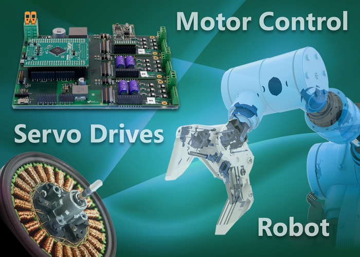
Factory Automation
Commercial Equipment
Consumer/PersonalIoT Equipment
Healthcare
Wearable Device
Mobile
Computer Peripherals
-
ProductsAutomotive Devices
Discrete Semiconductor
Diodes
Transistors
Logic ICs
Analog Devices
Digital Devices
Wireless Devices
※
 : Products list (parametric search)Power Semiconductors
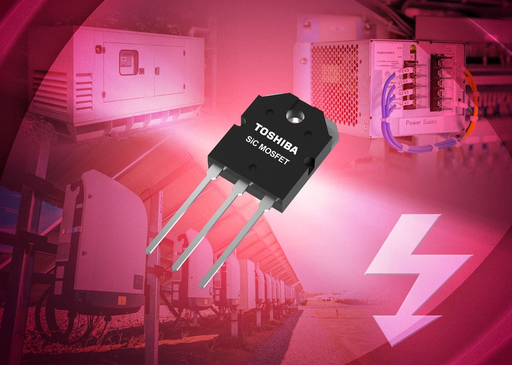
SiC Power Devices
※
: Products list (parametric search)Isolators/Solid State RelaysPhotocouplers
Digital Isolators
Solid State Relays
Fiber Optic Transmitting Modules
※
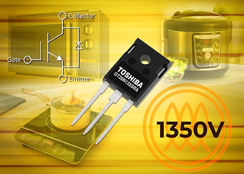
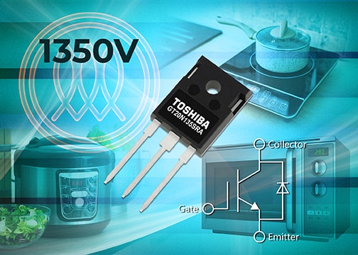
: Products list (parametric search)MOSFETsIGBTs/IEGTsBipolar Transistors※
: Products list (parametric search)Diodes※
: Products list (parametric search)MicrocontrollersMotor Driver ICsIntelligent Power ICs※
: Products list (parametric search)Power Management ICsLinear ICs※
: Products list (parametric search)General Purpose Logic ICsLinear Image SensorsOther Product ICsOther Product ICs
※
: Products list (parametric search) -
Design & Development
Design & Development
Innovation Centre
At the Toshiba Innovation Centre we constantly strive to inspire you with our technologies and solutions. Discover how to place us at the heart of your innovations.
-
Knowledge
Knowledge
Highlighted Topics
Further Materials
Other
- Where To Buy


- Part Number & Keyword Search
- Cross Reference Search
- Parametric Search
- Stock Check & Purchase
This webpage doesn't work with Internet Explorer. Please use the latest version of Google Chrome, Microsoft Edge, Mozilla Firefox or Safari.
require 3 characters or more. Search for multiple part numbers fromhere.
The information presented in this cross reference is based on TOSHIBA's selection criteria and should be treated as a suggestion only. Please carefully review the latest versions of all relevant information on the TOSHIBA products, including without limitation data sheets and validate all operating parameters of the TOSHIBA products to ensure that the suggested TOSHIBA products are truly compatible with your design and application.Please note that this cross reference is based on TOSHIBA's estimate of compatibility with other manufacturers' products, based on other manufacturers' published data, at the time the data was collected.TOSHIBA is not responsible for any incorrect or incomplete information. Information is subject to change at any time without notice.
require 3 characters or more.
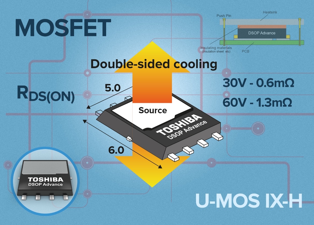
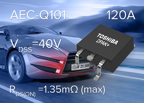
How to improve power conversion performance with new MOSFET technologies

To meet the demand for increasing energy efficiency in switching power conversion systems, superjunction MOSFETs have become preferred devices for energy-conscious designers. Superjunction technologies allow reduced die sizes enabling designers to reduce space and increase current density. However, new demands are coming to the fore, such as improved noise performance.
Reducing electromagnetic noise emission is desirable in high-end power supplies for equipment such as LCD TVs, LED lighting, medical power supplies, notebook power adapters and power supplies for tablets.
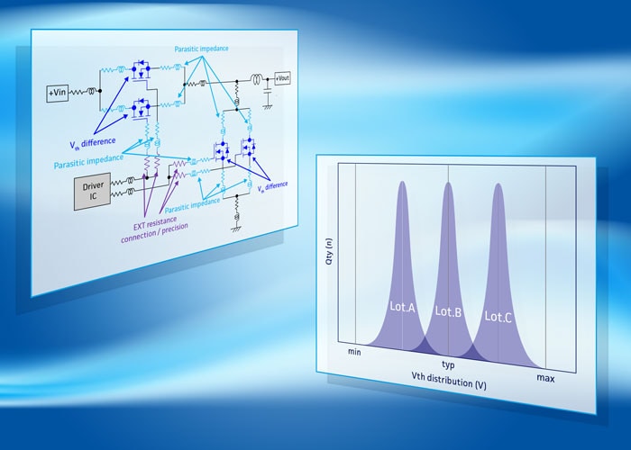
Toshiba's Deep Trench MOSFETs (DTMOS) devices have led the market in terms of performance for some time. The latest (fifth-generation) DTMOS V superjunction devices deliver a well-balanced ratio of lower noise and switching performance through a modified gate structure and patterning, resulting in increased reverse transfer capacitance between gate and drain (Crss or Cgd).
Emitted noise is comparable to competing low-EMI devices, while DTMOS V delivers the superior on-resistance that characterises superjunction technology. Fifth-generation N-channel, 0.38mΩ-class 600V devices used in a PFC circuit, show a significant EMI reduction.
The new devices bring other substantial benefits to power designers including a 30% improvement in the fundamental figure-of-merit (FOM) of on-resistance x chip size (Ron*A).
Also, the effects of temperature on RDS(ON) are reduced, ensuring more consistent performance. When compared to competitive devices and previous DTMOS generations, RDS(ON) is 15% lower, at high temperatures. Therefore costs can be saved through less simpler heat management.
The body diode achieves fast recovery times, even at high temperature, resulting in lower power losses, less heat generation and a more thermally efficient design.
The superjunction process also reduces the output capacitance, COSS, by 12%. This leads to a reduction in the waste energy being stored in the device that has to be dissipated during each and every switching cycle; making DTMOS ideal for the fast-switching and resonant topologies commonly found in power designs, even at partial load operation.
To find out how DTMOS V technology can help reduce EMI and improve performance of your power switching applications, please click here: