- General Top
- SEMICONDUCTOR
- STORAGE
- COMPANY
-
My ToshibaSemicon
- Semiconductor Top
-
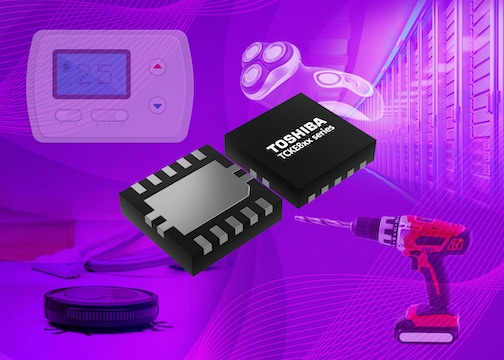
ApplicationsAutomotive
Body Electronics
xEV
In-Vehicle Infotainment
Advanced Driver-Assistance Systems (ADAS)
Chassis
IndustrialInfrastructure
BEMS/HEMS
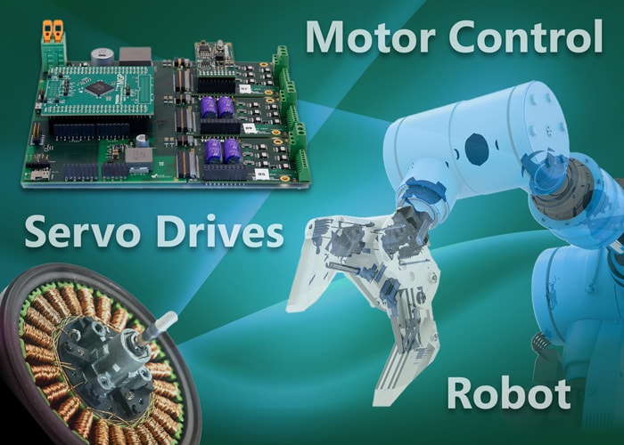
Factory Automation
Commercial Equipment
Consumer/PersonalIoT Equipment
Healthcare
Wearable Device
Mobile
Computer Peripherals
-
ProductsAutomotive Devices
Discrete Semiconductor
Diodes
Transistors
Logic ICs
Analog Devices
Digital Devices
Wireless Devices
※
 : Products list (parametric search)Power Semiconductors
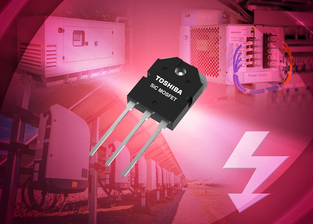
SiC Power Devices
※
: Products list (parametric search)Isolators/Solid State RelaysPhotocouplers
Digital Isolators
Solid State Relays
Fiber Optic Transmitting Modules
※
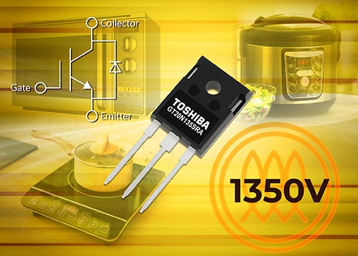
: Products list (parametric search)MOSFETsIGBTs/IEGTsBipolar Transistors※
: Products list (parametric search)Diodes※
: Products list (parametric search)MicrocontrollersMotor Driver ICsIntelligent Power ICs※
: Products list (parametric search)Power Management ICsLinear ICs※
: Products list (parametric search)General Purpose Logic ICsLinear Image SensorsOther Product ICsOther Product ICs
※
: Products list (parametric search) -
Design & Development
Design & Development
Innovation Centre
At the Toshiba Innovation Centre we constantly strive to inspire you with our technologies and solutions. Discover how to place us at the heart of your innovations.
-
Knowledge
Knowledge
Highlighted Topics
Further Materials
Other
- Where To Buy


- Part Number & Keyword Search
- Cross Reference Search
- Parametric Search
- Stock Check & Purchase
This webpage doesn't work with Internet Explorer. Please use the latest version of Google Chrome, Microsoft Edge, Mozilla Firefox or Safari.
require 3 characters or more. Search for multiple part numbers fromhere.
The information presented in this cross reference is based on TOSHIBA's selection criteria and should be treated as a suggestion only. Please carefully review the latest versions of all relevant information on the TOSHIBA products, including without limitation data sheets and validate all operating parameters of the TOSHIBA products to ensure that the suggested TOSHIBA products are truly compatible with your design and application.Please note that this cross reference is based on TOSHIBA's estimate of compatibility with other manufacturers' products, based on other manufacturers' published data, at the time the data was collected.TOSHIBA is not responsible for any incorrect or incomplete information. Information is subject to change at any time without notice.
require 3 characters or more.
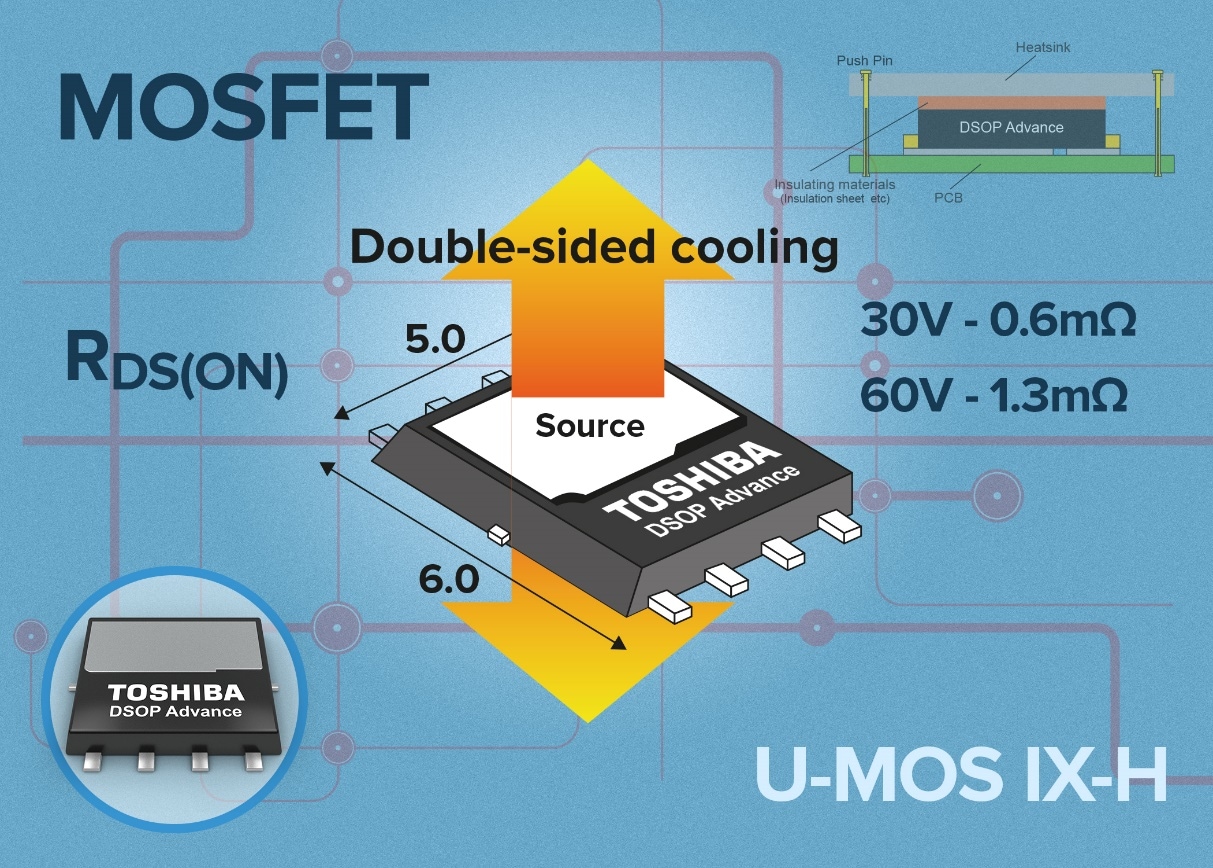
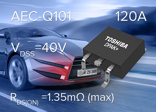
Why new superjunction developments are delivering cooler, more efficient MOSFETs

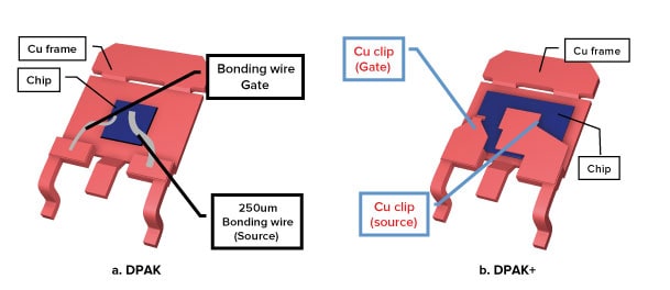
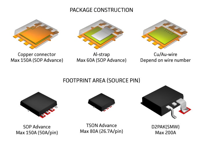
Superjunction MOSFETs have become favoured solutions for energy-conscious designers. Through semiconductor process advances, modern devices allow smaller die sizes for the same MOSFET on-resistance, enabling designers to reduce circuit size and increase current density.
Improved fabrication processes, such as the single-epitaxial fabrications enabled by deep trench filling, give greater freedom to optimise N- and P-channel aspect ratios thereby minimising on-resistance and reducing MOSFET size.
Toshiba’s fourth-generation DTMOS IV family takes advantage of single epitaxy to reduce on-resistance per die area by 30%. The latest DTMOS V is also based on the deep trench process, with additional cell structure improvements.
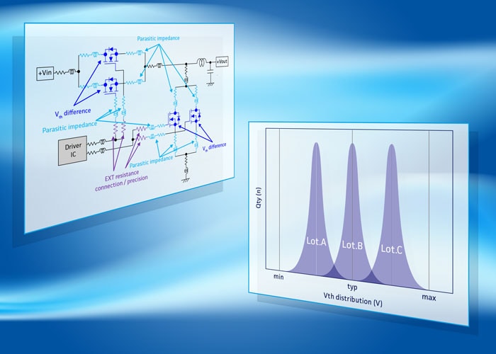
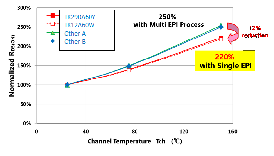
The single-epitaxial process enables superjunction MOSFETs to deliver more stable performance over the entire temperature change, addressing the efficiency reduction often experienced at higher operating temperatures. Single EPI devices can offer a 12% lower on-resistance (RDS(ON)) than multi EPI at 150°C. The resistance curve is also flatter, demonstrating more consistent performance.
The fifth-generation DTMOS V devices also display a well-balanced ratio of lower noise performance and switching performance, achieved through a modified gate structure and patterning.
Other substantial benefits to designers of power electronics include a figure-of-merit (FoM) of resistance x chip size that shows a 30% improvement over DTMOS III, leading to chips with lower values of RDS(ON) in the same package size.
DTMOS IV solutions with fast body diode offer recovery times in the region of 140ns, even at high temperature. This results in lower power losses, less heat generation and a more thermally efficient design. The superjunction process also reduces the output capacitance, COSS, by 12%, leading to a reduction in the waste energy being stored in the device (that has to be dissipated during each and every switching cycle). Which is why DTMOS is ideal for the fast-switching and resonant topologies commonly found in power designs.
Ultimately, the latest single epitaxy DTMOS devices simply generate less heat at the same performance levels as earlier devices. As less heat is generated, less heat has to be dissipated, thereby saving cost, space and weight by allowing for less stringent heat management requirements.
To learn more about the consistent and efficient performance of Toshiba's latest deep-trench MOSFETs, please click here.