- General Top
- SEMICONDUCTOR
- STORAGE
- COMPANY
-
My ToshibaSemicon
- Semiconductor Top
-
ApplicationsAutomotive
Body Electronics
xEV
In-Vehicle Infotainment
Advanced Driver-Assistance Systems (ADAS)
Chassis
IndustrialInfrastructure
BEMS/HEMS
Factory Automation
Commercial Equipment
Consumer/PersonalIoT Equipment
Healthcare
Wearable Device
Mobile
Computer Peripherals
-
ProductsAutomotive Devices
Discrete Semiconductor
Diodes
Transistors
Logic ICs
Analog Devices
- Automotive SmartMCD™ (Integreted SoC Conbining Microcontroller and Driver)
- Automotive Brushless Motor Driver ICs
- Automotive Brushed DC Motor Driver ICs
- Automotive Stepping Motor Driver ICs
- Automotive Driver ICs
- Automotive System Power Supplies ICs
- Automotive audio power amplifier ICs
- Automotive Network Communication
Digital Devices
Wireless Devices
※
 : Products list (parametric search)Power Semiconductors
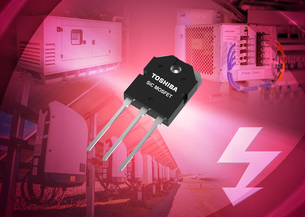
SiC Power Devices
※
: Products list (parametric search)Isolators/Solid State RelaysPhotocouplers
Digital Isolators
Solid State Relays
Fiber Optic Transmitting Modules
※
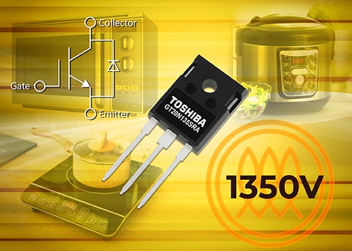
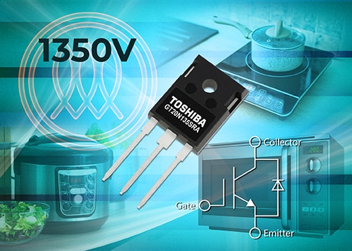
: Products list (parametric search)MOSFETsIGBTs/IEGTsBipolar Transistors※
: Products list (parametric search)Diodes※
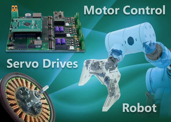
: Products list (parametric search)MicrocontrollersMotor Driver ICsIntelligent Power ICs※
: Products list (parametric search)Power Management ICsLinear ICs※
: Products list (parametric search)General Purpose Logic ICsLinear Image SensorsOther Product ICsOther Product ICs
※
: Products list (parametric search) -
Design & Development
Design & Development
Innovation Centre
At the Toshiba Innovation Centre we constantly strive to inspire you with our technologies and solutions. Discover how to place us at the heart of your innovations.
-
Knowledge
Knowledge
Highlighted Topics
Further Materials
Other
- Where To Buy


- Part Number & Keyword Search
- Cross Reference Search
- Parametric Search
- Stock Check & Purchase
This webpage doesn't work with Internet Explorer. Please use the latest version of Google Chrome, Microsoft Edge, Mozilla Firefox or Safari.
require 3 characters or more. Search for multiple part numbers fromhere.
The information presented in this cross reference is based on TOSHIBA's selection criteria and should be treated as a suggestion only. Please carefully review the latest versions of all relevant information on the TOSHIBA products, including without limitation data sheets and validate all operating parameters of the TOSHIBA products to ensure that the suggested TOSHIBA products are truly compatible with your design and application.Please note that this cross reference is based on TOSHIBA's estimate of compatibility with other manufacturers' products, based on other manufacturers' published data, at the time the data was collected.TOSHIBA is not responsible for any incorrect or incomplete information. Information is subject to change at any time without notice.
require 3 characters or more.
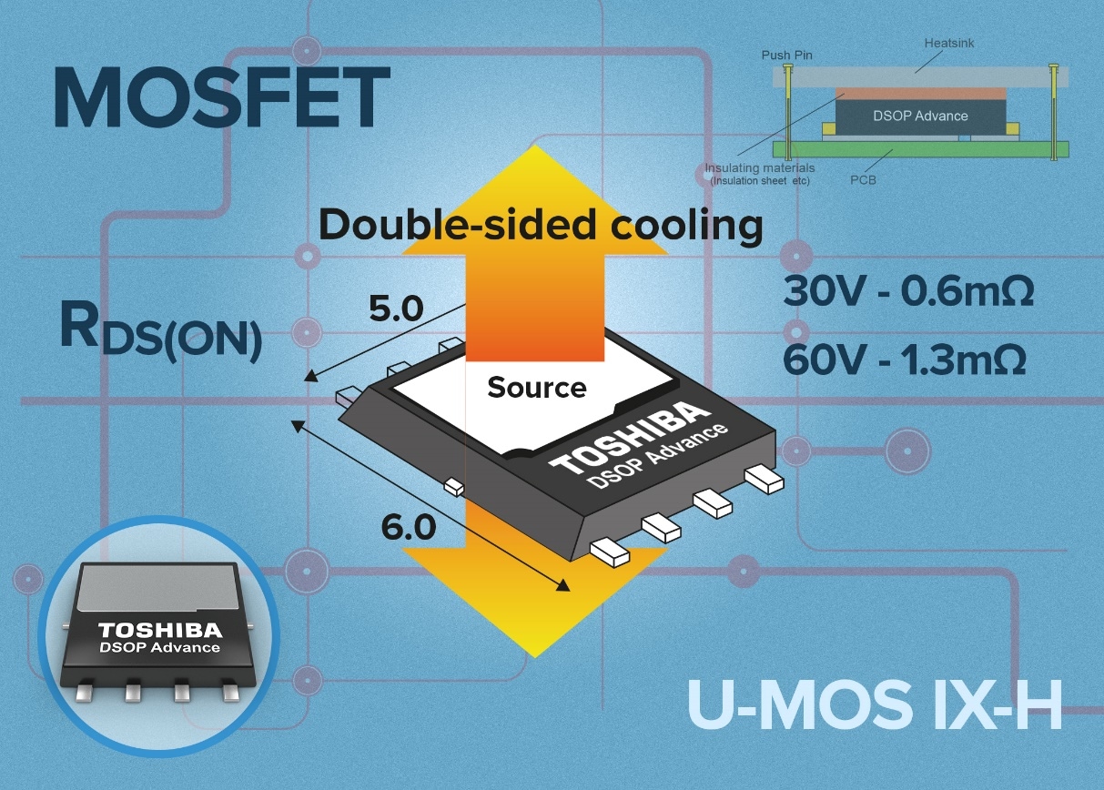
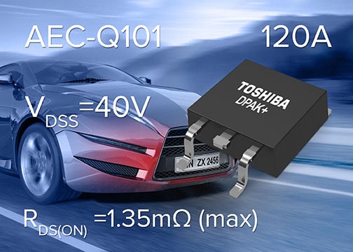
Superjunction MOSFET Technology Trends for Power Design

Smaller package sizes and increased power density levels are the order of the day in circuit designs intended for power conversion. They are just one of a broad range of pressures being exerted onto electronics engineers, however. Energy efficiency and operational reliability are two equally significant demands, along with cost constraints.
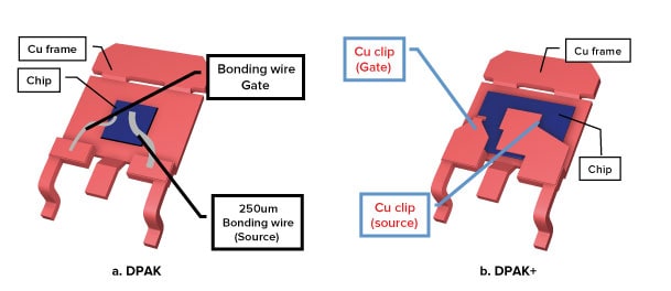
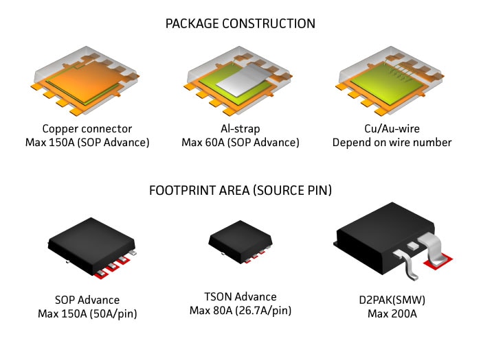
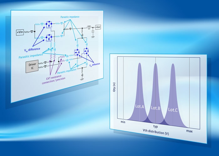
Power MOSFETs find wide employment in the switching and amplifying of electronic signals. They are the most commonly used low voltage (sub 200V) switches, but have drawbacks when switching rapidly at higher voltages. Superjunction MOSFETs were developed to help alleviate such problems. They offer reductions in a variety of different areas - including die size, which has a direct influence on device cost. However, they still require close attention to be paid to the system design, particularly in terms of reducing PCB parasitics.
For MOSFETs rated at 600V, more than 95% of the device resistance comes directly from the epitaxial layer. The objective of developing superjunction MOSFETs was to overcome this, using techniques such as deep trench filling.
This is exemplified in the latest generation DTMOS V devices from Toshiba. These are based on a single epitaxial process, rather than the multi-epitaxial process of earlier devices. As a consequence, they offer significant reductions in RDS(ON) (a 17% improvement) and lower EMI noise over the previous fourth generation devices.
The combination of superjunction MOSFETs and Schottky barrier diodes with silicon carbide (SiC) construction is proving to be tremendously helpful to engineers implementing power conversion systems - allowing them to reduce circuit size at the same time as increasing current density. Other advantages of using superjunction MOSFETs over more conventional planar silicon devices are the lowering of conduction losses for a given die size, the curbing of switching losses and reduced heat generation (thus simplifying the thermal management requirements). A further benefit is in relation to improved noise performance - as low EMI noise is increasingly expected from the power sources of applications as diverse as consumer goods, LED lighting, medical power supplies, notebook/tablet adapters.
You can find out more about Toshiba’s DTMOS V MOSFET technology and operational advantages when used in conjunction with SiC diode devices by downloading Toshiba’s white paper: