
- 半導體首頁
-
應用Automotive
Body Electronics
xEV
In-Vehicle Infotainment
Advanced Driver-Assistance Systems (ADAS)
Chassis
IndustrialInfrastructure
BEMS/HEMS
Factory Automation
Commercial Equipment
Consumer/PersonalIoT Equipment
Healthcare
Wearable Device
Mobile
Computer Peripherals
-
產品車用元件
Discrete Semiconductor
Diodes
電晶體
通用邏輯IC
Analog Devices
Digital Devices
Wireless Devices
※
 : Products list (parametric search)功率半導體
※
: Products list (parametric search)隔離器/固態繼電器Photocouplers
Digital Isolators
※
: Products list (parametric search)MOSFETsIGBTs/IEGTs雙極性電晶體※
: Products list (parametric search)Diodes※
: Products list (parametric search)微控制器馬達驅動 ICs智能功率 ICs※
: Products list (parametric search)電源管理 ICs線性 ICs※
: Products list (parametric search)通用邏輯 ICs線性影像感測器其他產品其他產品
※
: Products list (parametric search) -
開發/設計支援
開發 / 設計支援
-
技術知識
- 購買管道


- 型號 & 關鍵字搜尋
- 交叉搜尋
- 參數搜尋
- 線上庫存查詢跟購買
This webpage doesn't work with Internet Explorer. Please use the latest version of Google Chrome, Microsoft Edge, Mozilla Firefox or Safari.
型號需要超過三個文字以上 Search for multiple part numbers fromhere.
The information presented in this cross reference is based on TOSHIBA's selection criteria and should be treated as a suggestion only. Please carefully review the latest versions of all relevant information on the TOSHIBA products, including without limitation data sheets and validate all operating parameters of the TOSHIBA products to ensure that the suggested TOSHIBA products are truly compatible with your design and application.Please note that this cross reference is based on TOSHIBA's estimate of compatibility with other manufacturers' products, based on other manufacturers' published data, at the time the data was collected.TOSHIBA is not responsible for any incorrect or incomplete information. Information is subject to change at any time without notice.
型號需要超過三個文字以上
2-3. Conductivity modulation
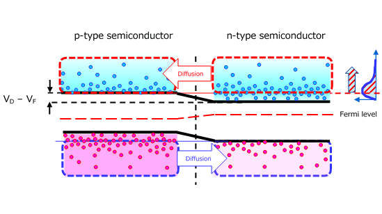
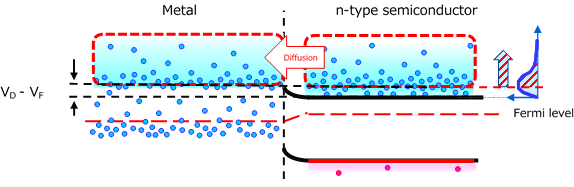
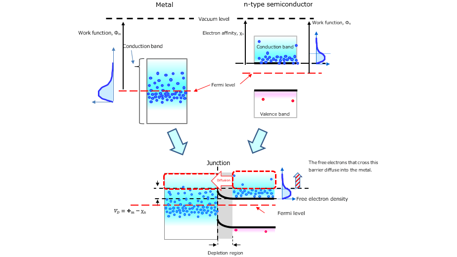
In the previous subsections, we have discussed the pn and metal-semiconductor junctions. A pn junction is a bipolar junction because both electrons and holes act as charge carriers whereas a metal-semiconductor junction is a unipolar junction (also called a monopolar junction) because either electrons or holes act as charge carriers.
To create a pn junction, a lightly doped n-type (or p-type) semiconductor substrate is heavily doped with boron (B) or other p-type dopant using a diffusion, epitaxial growth, or ion implantation process. Therefore, the lightly doped n-type (or p-type) substrate acts as a series resistor. Note that the conductivity modulation of the pn junction causes its series resistance to decrease.
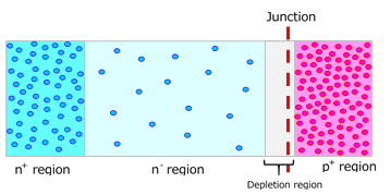
Typical pn junction diodes consist of heavily doped p-type (p+) and n-type (n+) regions on either side of a lightly doped n (n–) region. Diodes with an extremely lightly doped n– region are called PIN diodes. Typical pn junction diodes have a structure similar to that of PIN diodes although I layers of pn junction diodes are more heavily doped.
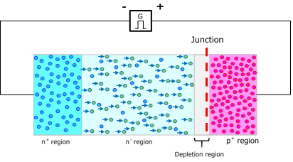
Electrons from a power supply flow into the n– region via the n+ region. To maintain electrical neutrality, holes are injected into the n– region from the p+ region. These electrons and holes recombine and disappear ultimately. Carrier lifetime is defined as the average time required for this recombination. Because both electrons and holes exist in the n– region during this period, it exhibits low resistance as if it were a heavily doped region.
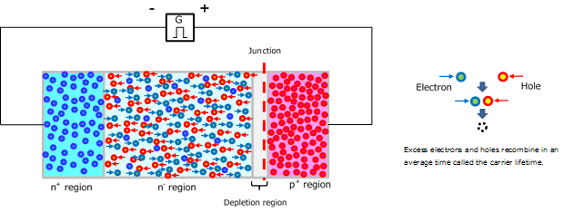
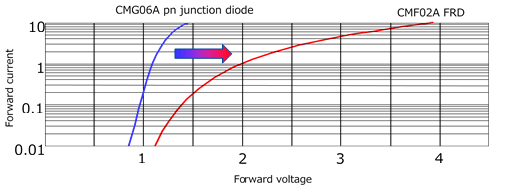
The longer the carrier lifetime, the stronger the conductivity modulation effect, yet at the expense of an increase in reverse recovery time (i.e., the time required for a diode to stop conducting). Toshiba provides a type of diodes with a reduced reverse recovery time (i.e., a reduced carrier lifetime) called fast-recovery diodes (FRDs). The FRD has a shallower forward voltage-vs-forward current curve (i.e., higher forward resistance) than the typical pn junction diode as shown in Figure 2-10.
- Prev
- 4/4
Chapter2 Basics of Schottky Barrier Diodes (Basic of Metal-semiconductor junction)


Related information
- Products
Schottky Barrier Diodes - Application Notes
Application Notes - FAQs
Diodes - Parametric Search
Schottky Barrier Diodes - Stock Check & Purchase
Stock Check & Purchase