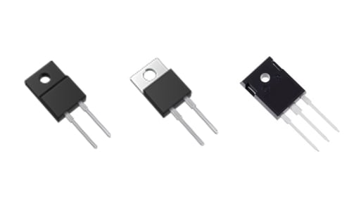
SiC Schottky Barrier Diodes (SiC肖特基勢壘二極體)

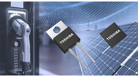
SiC肖特基勢壘二極體(SBD)具有較高的反向額定電壓。除了具有短反向恢復時間(t rr )的SBD,東芝還提供具有結勢壘肖特基(JBS)結構的650-V SBD,該結構提供低洩漏電流(I r ) 和開關模式電源所需的高浪湧電流能力。這些設備有助於提高開關電源的效率。

產品陣容

You can narrow down the search for applicable products by selecting specifications.

VRRM (Max) (V)
IF(DC) (Max) (A)
Number of Circuits
Package name (Toshiba)
VF (Max) (V)
Results:

You can narrow down your search for applicable products by package type or number of pins.

unit:

All package dimensions are guaranteed in millimeters as mentioned on datasheet. Package dimension in inches is round to 2 significant digits converted with 1mm=0.0393701inch.

About information presented in this cross reference

The information presented in this cross reference is based on TOSHIBA's selection criteria and should be treated as a suggestion only. Please carefully review the latest versions of all relevant information on the TOSHIBA products, including without limitation data sheets and validate all operating parameters of the TOSHIBA products to ensure that the suggested TOSHIBA products are truly compatible with your design and application.
Please note that this cross reference is based on TOSHIBA's estimate of compatibility with other manufacturers' products, based on other manufacturers' published data, at the time the data was collected.
TOSHIBA is not responsible for any incorrect or incomplete information. Information is subject to change at any time without notice.

3rd generation SiC Schottky barrier diode (SBD)
It adopts the new schottky metal, and it is equipped with 3rd generation SiC SBD chip, which optimized junction barrier schottky (JBS) structure of 2nd generation. As a result, we have achieved industry-leading lowest forward voltage 1.2 V (Typ.), which is 17 % lower than that of the 2nd generation 1.45 V (Typ.). The 3rd generation products have improved the trade-offs between forward voltage and total capacitive charge, and the trade-offs between forward voltage and reverse current compared with the 2nd generation products. This reduces power dissipation and contributes to high efficiency of equipment.
3rd generation SiC Schottky barrier diode (SBD)
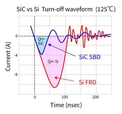
SiC SBD that achieves low switching losses
By using SiC, a device with high withstand voltage and low switching loss (low reverse recovery charge) has been realized.
Diodes / SiC Schottky Barrier Diodes
Contributes to high efficiency and low loss of high output power supply
Significantly reduced recovery loss compared to FRD: fast recovery diodes
Diodes / SiC Schottky Barrier Diodes
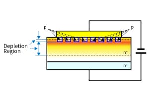
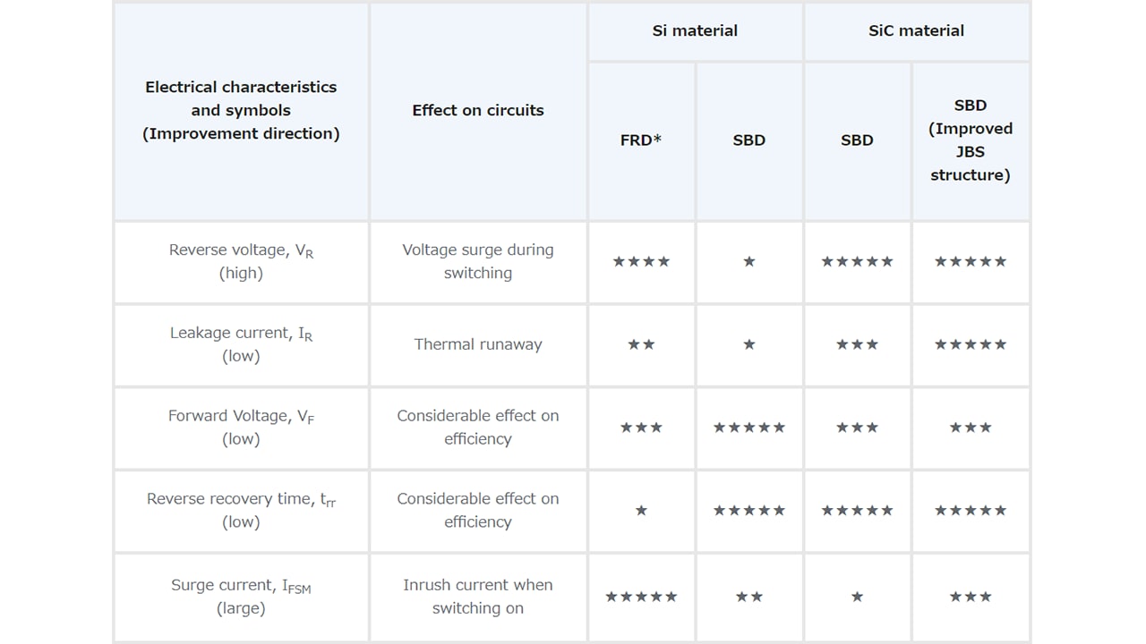
Improved JBS structure to reduce the leakage current and increase the surge current capability
The improved JBS structure has been applied to improve the leakage current of the SBD and the surge current capacity.
Diodes / SiC Schottky Barrier Diodes
SiC devices suitable for power supply circuits
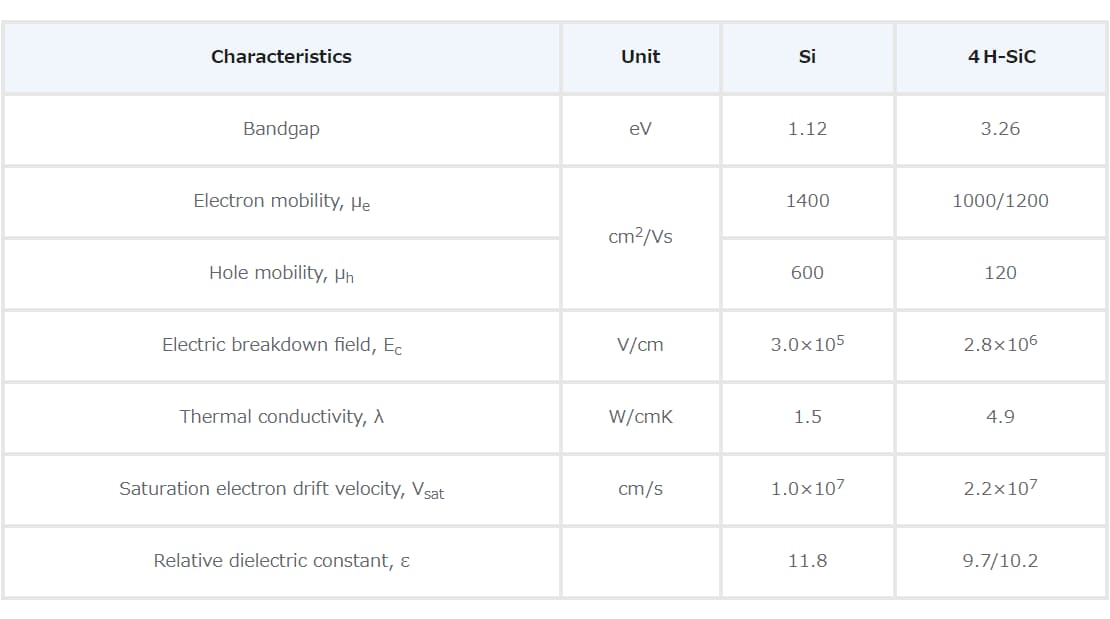
SiC Schottky barrier diodes (SBDs) have achieved high breakdown voltages for SBDs, which are difficult to achieve with Si materials, and significantly reduced reverse-recovery times (charges) that could not be achieved with p-n junction diodes, such as Si-FRD(Fast Recovery Diode).
Diodes / SiC Schottky Barrier Diodes
High withstand voltage (reverse voltage) characteristics of SiC SBDs
A device with a high breakdown voltage has been realized with dielectric breakdown field strength nearly 10 times higher than that of Si.
Diodes / SiC Schottky Barrier Diodes

文件下載

應用

Inverter/Servo
Such as low power consumption, miniaturization and robust operation are important in designing inverter/servo. Toshiba provides information on a wide range of semiconductor products suitable for power supply unit, motor driving circuit units, signal transmission units, etc., along with circuit configuration examples.
Thermostat
Such as low power consumption and miniaturization are important in designing thermostat. Toshiba provides information on a wide range of semiconductor products suitable for power supply units, isolation units, sensor signal input units, etc., along with circuit configuration examples.
Server
Such as low power consumption and miniaturization are important in designing server. Toshiba provides information on a wide range of semiconductor products suitable for power supply units, motor driving unit, over temperature monitoring unit, etc., along with circuit configuration examples.
Uninterruptible power supply
Such as low power consumption and miniaturization are important in designing uninterruptible power supply (UPS). Toshiba provides information on a wide range of semiconductor products suitable for power sullpy units, inverter/converter units, control units, signal transmission units, etc., along with circuit configuration examples.
Microwave Oven
Such as low noise, low power consumption and miniaturization are important in designing microwave oven. Toshiba provides information on a wide range of semiconductor products suitable for power supply unit, magnetron driving circuit units, sensor signal input units, etc., along with circuit configuration examples.

參考設計

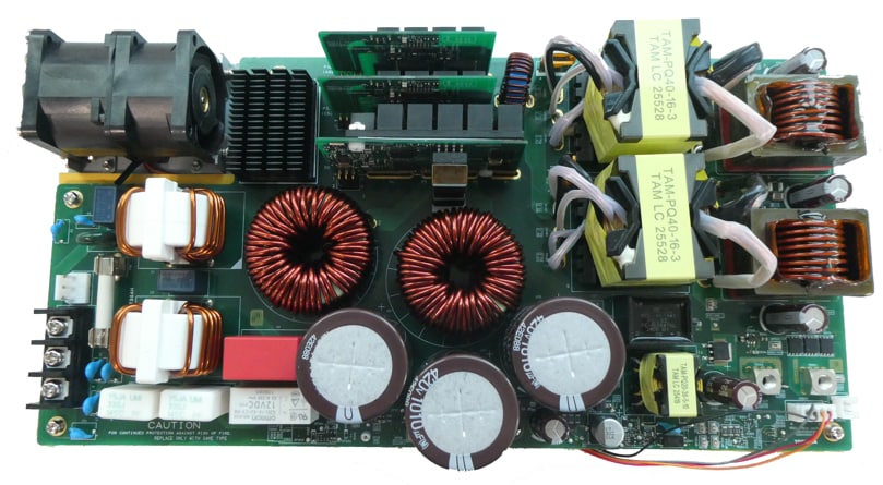
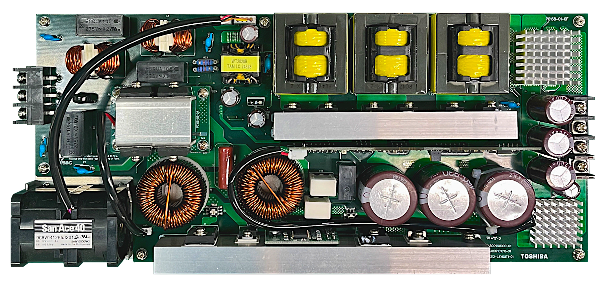
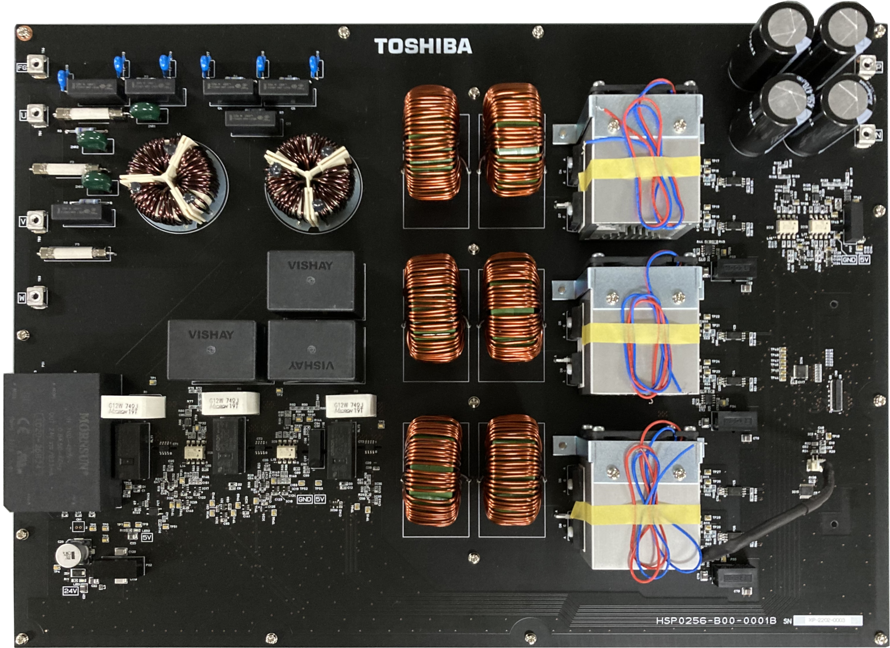
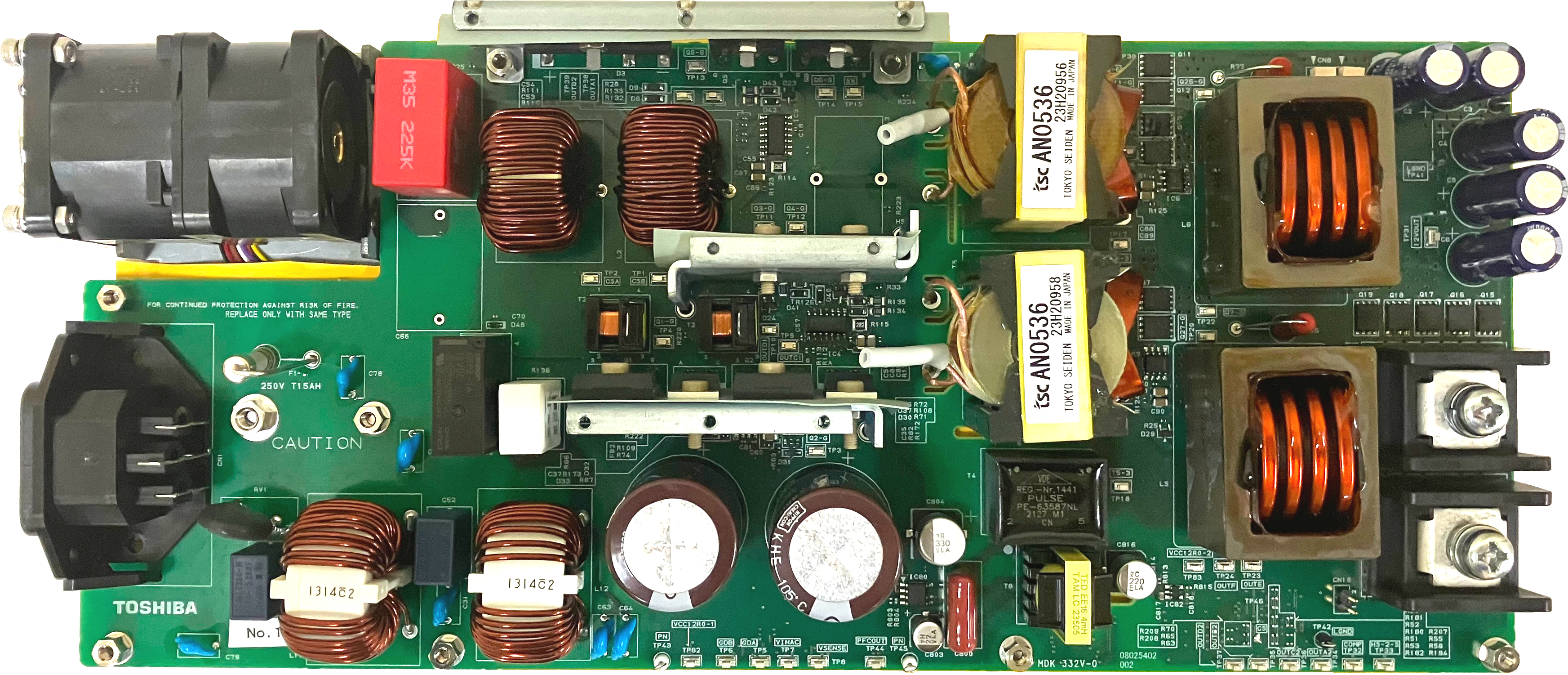
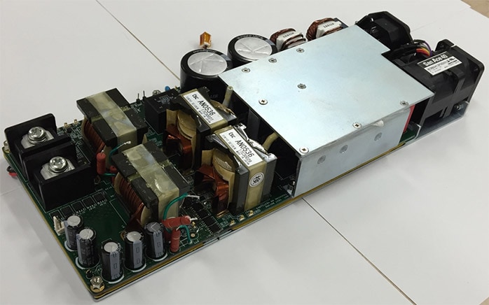
PCB Photo (example)
1.6 kW Server Power Supply (Upgraded)
Thanks to Toshiba’s latest power devices and digital isolator, this 1U size and 12 V output 1.6 kW server power supply achieves higher efficiency at whole load than the existing reference design which uses the same circuit topology. Design files and guides for circuit design and operation are available as reference design.
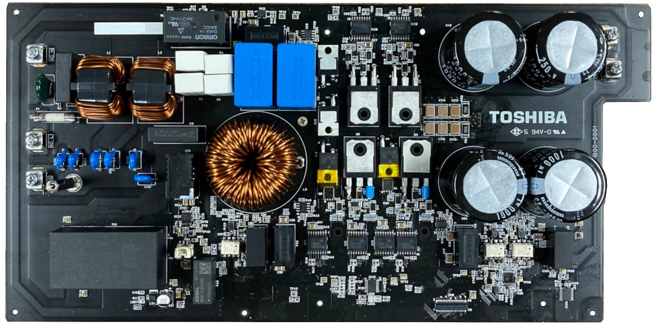
1.6 kW T-Type 3-Level PFC Power Supply
1.6kW T-Type 3-Level PFC電源
1.6kW AC-DC轉換器電源,具有T-Type 3-Level功率因數校正(PFC)電路。對各種電路的設計要點、設計數據、使用方法等進行說明。
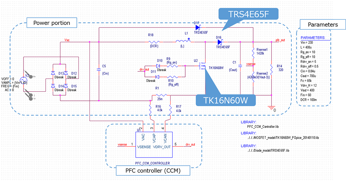
Circuit diagram of single phase PFC power supply basic simulation circuit.
Single Phase PFC Power Supply Basic Simulation Circuit
This reference design provides OrCAD® based simulation circuit, simulation results and design guide. This is for designing single phase PFC power supply.
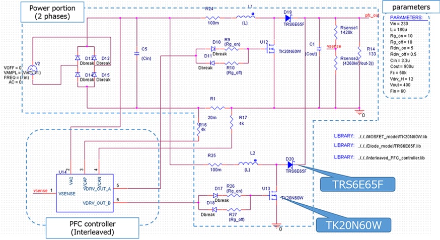
Circuit diagram of interleaved PFC power supply basic simulation circuit.
Interleaved PFC Power Supply Basic Simulation Circuit
This reference design provides OrCAD® based simulation circuit, simulation results and design guide. This is for designing interleaved PFC power supply.
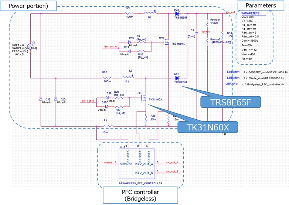
Circuit diagram of bridgeless PFC power supply basic simulation circuit.
Bridgeless PFC Power Supply Basic Simulation Circuit
This reference design provides OrCAD® based simulation circuit, simulation results and design guide. This is for designing bridgeless PFC power supply.
Features of 1.6kW, 80Plus Platinum class, high efficiency server AC-DC power supply .
1.6kW, 80Plus Platinum Class, High efficiency Server AC-DC Power supply
This reference design provides design guide, data and other contents of 1.6kW 80Plus Platinum class power supply using Semi-bridgeless/Isolated phase shift full bridge.

Simulation

聯繫我們

技術方面問題

聯絡我們

聯絡我們

常見問題

常見問答

採購 / 樣品 / IC可靠度 相關問題

線上庫存查詢跟購買

keyword:

Disclaimer for External Link
Through this website you are able to proceed to the website of our distributors ("Third Party Website") which is not under the control of Toshiba Corporation and its subsidiaries and affiliates (collectively "Toshiba"). The Third Party Website is made available to you as a convenience only and you agree to use the Third Party Website at your own risk. The link of the Third Party Website does not necessarily imply a recommendation or an endorsement by Toshiba of the Third Party Website. Please be aware that Toshiba is not responsible for any transaction done through the Third Party Website, and such transactions shall be subject to terms and conditions which may be provided in the Third Party Website.
開啟新視窗