-
My ToshibaSemicon
- 網站首頁 檢視
-
半導體 檢視
-
應用
Body Electronics
xEV
In-Vehicle Infotainment
Advanced Driver-Assistance Systems (ADAS)
Chassis
Infrastructure
BEMS/HEMS
Factory Automation
Commercial Equipment
IoT Equipment
Healthcare
Wearable Device
Mobile
Computer Peripherals
-
產品
*
: Products list (parametric search)
Photocouplers
Digital Isolators
*
: Products list (parametric search)
*
: Products list (parametric search)
*
: Products list (parametric search)
*
: Products list (parametric search)
Discrete Semiconductor
Diodes
電晶體
通用邏輯IC
Analog Devices
Digital Devices
Wireless Devices
*
: Products list (parametric search)
*
: Products list (parametric search)
*
: Products list (parametric search)
*
: Products list (parametric search)
-
開發/設計支援
-
技術知識
- 購買管道 檢視
-
- 儲存產品 檢視
- 公司資訊 檢視
- 型號查詢
- 交叉搜尋
- 關鍵字搜尋
- 參數搜尋
- 線上庫存查詢跟購買
This webpage doesn't work with Internet Explorer. Please use the latest version of Google Chrome, Microsoft Edge, Mozilla Firefox or Safari.
型號需要超過三個文字以上
The information presented in this cross reference is based on TOSHIBA's selection criteria and should be treated as a suggestion only. Please carefully review the latest versions of all relevant information on the TOSHIBA products, including without limitation data sheets and validate all operating parameters of the TOSHIBA products to ensure that the suggested TOSHIBA products are truly compatible with your design and application.Please note that this cross reference is based on TOSHIBA's estimate of compatibility with other manufacturers' products, based on other manufacturers' published data, at the time the data was collected.TOSHIBA is not responsible for any incorrect or incomplete information. Information is subject to change at any time without notice.
型號需要超過三個文字以上
What is the maximum voltage that can be applied to the base of a bias resistor built-in transistor (BRT)? (How many watts is the allowable power dissipation of the built-in resistors?)

You do not need to consider the maximum allowable base voltage for typical applications (in which input voltage (VI) is lower than 10 V), but care is required when VI is higher than 10 V.
The maximum input voltage (VI) is mainly determined by the following factors:
1. Value of the series base resistor (R1) (i.e., the power dissipated by R1)
2. Maximum collector current (IC)
The maximum input voltage varies with the usage conditions of a BRT (e.g., hFE), but it is generally determined by the collector current when the R1 value is small and by the R1 value when it is large.
1. Relationship between the value of the series base resistor (R1) and the input voltage (VI)
The allowable power dissipation of the built-in resistors of a BRT is 1/8 W. Let the base-emitter voltage of the internal transistor in the “on” state be Vbe. Then, the current flowing through R1 (IB) is expressed as follows. For the sake of simplicity, let Vbe = 0.7 V.
IB = ( VI – Vbe ) / R1 = ( VI – 0.7 ) / R1
The power dissipation of R1 due to IB must not exceed 1/8 W. Hence:
1/8 W > R1 * { ( VI – 0.7 ) / R1 }^2
> ( VI – 0.7 ) ^2 / R1
VI < √( R1 / 8 ) + 0.7
2. Relationship between the maximum collector current (IC(max)) and the input voltage (VI)
The maximum collector current (IC(max)) is specified as an absolute maximum rating, which must not be exceeded even instantaneously.
Since the BRT operates in the saturation region, its hFE is in the range of 10 to 20. The current flowing to the base (b) of the internal transistor (Ib) can be calculated by subtracting the current flowing to R2 (IR2) from the IB value calculated above:
Ib = IB – IR2 = ( VI – Vbe ) / R1 – Vbe / R2 = ( VI – 0.7 ) / R1 – 0.7 / R2
Since the collector current (IC) is equal to Ib times hFE, the following equation must be satisfied:
IC (max) > IC = hFE * IB = hFE * {( VI – 0.7 ) / R1 – 0.7 / R2 }
VI < R1 * IC(max) / hFE +( R1 + R2 ) * 0.7 / R2
The lower of the VI values calculated based on the above two factors is the maximum allowable base voltage.
1. Value of the series base resistor (R1)
VI < √( R1 / 8 ) + 0.7
2. Maximum collector current (IC(max))
VI < R1 * IC (max) / hFE +( R1 + R2 ) * 0.7 / R2
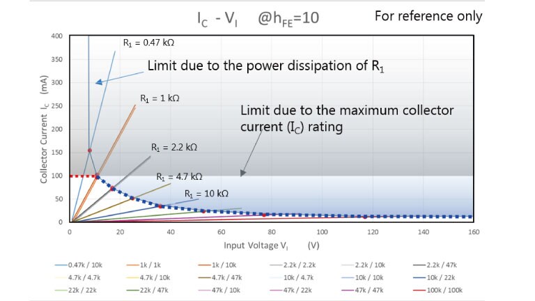
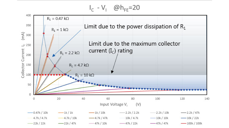
Figure 2 and Figure 3 show the relationships between input voltage and collector current at different resistor values.
Although the maximum input voltage and its limiting factors depend on the hFE (IC/IB) of the BRT, the following are true:
- When the R1 value is small: The maximum input voltage is determined by the absolute maximum collector current specified in the datasheet.
- When the R1 value is large: The maximum input voltage is determined by the power dissipation of R1.


