
- 半導體首頁
-
應用Automotive
Body Electronics
xEV
In-Vehicle Infotainment
Advanced Driver-Assistance Systems (ADAS)
Chassis
IndustrialInfrastructure
BEMS/HEMS
Factory Automation
Commercial Equipment
Consumer/PersonalIoT Equipment
Healthcare
Wearable Device
Mobile
Computer Peripherals
-
產品車用元件
Discrete Semiconductor
Diodes
電晶體
通用邏輯IC
Analog Devices
Digital Devices
Wireless Devices
※
 : Products list (parametric search)功率半導體
※
: Products list (parametric search)隔離器/固態繼電器Photocouplers
Digital Isolators
※
: Products list (parametric search)MOSFETsIGBTs/IEGTs雙極性電晶體※
: Products list (parametric search)Diodes※
: Products list (parametric search)微控制器馬達驅動 ICs智能功率 ICs※
: Products list (parametric search)電源管理 ICs線性 ICs※
: Products list (parametric search)通用邏輯 ICs線性影像感測器其他產品其他產品
※
: Products list (parametric search) -
開發/設計支援
開發 / 設計支援
-
技術知識
- 購買管道


- 型號 & 關鍵字搜尋
- 交叉搜尋
- 參數搜尋
- 線上庫存查詢跟購買
This webpage doesn't work with Internet Explorer. Please use the latest version of Google Chrome, Microsoft Edge, Mozilla Firefox or Safari.
型號需要超過三個文字以上 Search for multiple part numbers fromhere.
The information presented in this cross reference is based on TOSHIBA's selection criteria and should be treated as a suggestion only. Please carefully review the latest versions of all relevant information on the TOSHIBA products, including without limitation data sheets and validate all operating parameters of the TOSHIBA products to ensure that the suggested TOSHIBA products are truly compatible with your design and application.Please note that this cross reference is based on TOSHIBA's estimate of compatibility with other manufacturers' products, based on other manufacturers' published data, at the time the data was collected.TOSHIBA is not responsible for any incorrect or incomplete information. Information is subject to change at any time without notice.
型號需要超過三個文字以上
pn Junction
Download "Chapter I : Basis of Semiconductors" (PDF:1.2MB)
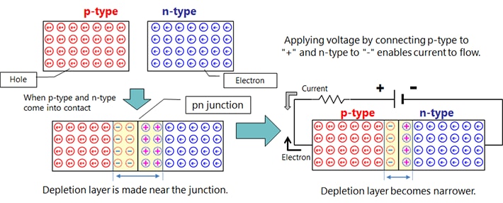
The interface between a p-type semiconductor and an n-type semiconductor is called a pn junction. When a p-type semiconductor and an n-type semiconductor are joined (not actually joined, but formed by doping so that they are adjacent to each other), the carriers, holes and free electrons, are attracted to each other and combine and disappear near the boundary. Since there are no carriers in this area, it is called a depletion layer and is in the same state as an insulator. (No bias state)
- Forward direction (connect the positive pole to the p-type region and the negative pole to the n-type region and apply voltage):
When the applied voltage is gradually increased and exceeds the forward voltage (about 0.7V for Si), electrons flow one after another from the n-type region to the p-type region, and electrons that do not combine with holes and disappear move to the positive pole, allowing current to flow. For an explanation of the physical properties of a pn junction, see the following e-learning.
Basics of Schottky Barrier Diodes 1-3. pn junction
- Reverse direction (connect the negative pole to the p-type region and the positive pole to the n-type region and apply voltage):
No current flows. In the normal voltage range, the excess electrons in the n-type semiconductor move away from the boundary surface. The holes in the p-type semiconductor also move away from the boundary surface. This causes the depletion layer near the boundary surface to expand. However, if a voltage exceeding the breakdown voltage is applied, the pn junction enters a breakdown state due to the Zener effect (avalanche effect) and current flows suddenly. In a typical diode, this breakdown causes the performance to deteriorate and be destroyed.
Chapter I : Basis of Semiconductors

Related information
- Products
- FAQ