
- 半導體首頁
-
應用Automotive
Body Electronics
xEV
In-Vehicle Infotainment
Advanced Driver-Assistance Systems (ADAS)
Chassis
IndustrialInfrastructure
BEMS/HEMS
Factory Automation
Commercial Equipment
Consumer/PersonalIoT Equipment
Healthcare
Wearable Device
Mobile
Computer Peripherals
-
產品車用元件
Discrete Semiconductor
Diodes
電晶體
通用邏輯IC
Analog Devices
Digital Devices
Wireless Devices
※
 : Products list (parametric search)功率半導體
※
: Products list (parametric search)隔離器/固態繼電器Photocouplers
Digital Isolators
※
: Products list (parametric search)MOSFETsIGBTs/IEGTs雙極性電晶體※
: Products list (parametric search)Diodes※
: Products list (parametric search)微控制器馬達驅動 ICs智能功率 ICs※
: Products list (parametric search)電源管理 ICs線性 ICs※
: Products list (parametric search)通用邏輯 ICs線性影像感測器其他產品其他產品
※
: Products list (parametric search) -
開發/設計支援
開發 / 設計支援
-
技術知識
- 購買管道


- 型號 & 關鍵字搜尋
- 交叉搜尋
- 參數搜尋
- 線上庫存查詢跟購買
This webpage doesn't work with Internet Explorer. Please use the latest version of Google Chrome, Microsoft Edge, Mozilla Firefox or Safari.
型號需要超過三個文字以上 Search for multiple part numbers fromhere.
The information presented in this cross reference is based on TOSHIBA's selection criteria and should be treated as a suggestion only. Please carefully review the latest versions of all relevant information on the TOSHIBA products, including without limitation data sheets and validate all operating parameters of the TOSHIBA products to ensure that the suggested TOSHIBA products are truly compatible with your design and application.Please note that this cross reference is based on TOSHIBA's estimate of compatibility with other manufacturers' products, based on other manufacturers' published data, at the time the data was collected.TOSHIBA is not responsible for any incorrect or incomplete information. Information is subject to change at any time without notice.
型號需要超過三個文字以上
What is an ESD protection diode?
An ESD protection diode is a type of Zener diode optimized for ESD protection applications.
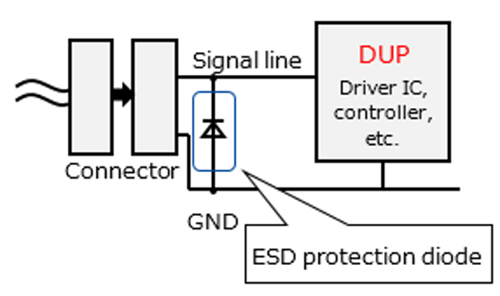
It is used to protect an IC from excessive voltage (e.g., ESD) higher than the rated withstand voltage that enters a board via an externally exposed port such as a USB port. ESD protection diodes are also called transient voltage suppressor (TVS) diodes. A slight difference between them is that the term “TVS diodes” refers to a wider range of diodes that are designed to provide protection not only from ESD strikes but also from lightning surges, switching surges, and typical signal ripples. Toshiba’s product portfolio also provides diodes for switching surge protection.
(See “Zener diode for overvoltage protection.”)
In the absence of ESD during normal operation, ESD protection diodes are invisible to a system. They are designed to conduct in the event of an excessive ESD event in order to protect an IC. In the past, Zener diodes were used for this application.
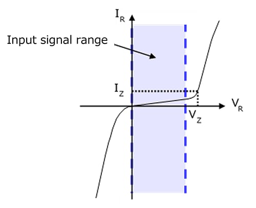
A Zener diode is a type of pn junction diode designed to be used in reverse bias. As the reverse voltage across a pn junction diode is increased, avalanche breakdown occurs at some point called Zener voltage (VZ). The Zener voltage is hardly dependent on the current flowing through the Zener diode. Therefore, Zener diodes can be used to provide a fixed reference voltage although they are seldom used for this application nowadays. Because of this characteristic, Zener diodes are also called voltage regulator diodes. The desired Zener voltage can be obtained by optimizing the dopant densities of the p-type and n-type regions that form the pn junction.
Toshiba provides an extensive lineup of Zener diodes with different Zener voltages.
To use Zener diodes for ESD protection, select ones that satisfy
0< VIN < VZ*.
Generally, the diodes that are used for ESD protection are inserted between ground and an I/O line that could be exposed to ESD. The following summarizes the characteristics required for these diodes:
- ESD protection diodes should neither conduct in normal operation nor affect the signal integrity of the line.
- Standardization of the range of voltage in which an ESD protection diode does not conduct
- Reduction in total capacitance
- In the event of excessive voltage being applied to a signal line, ESD protection diodes should not only turn on but also minimize the voltage and current applied to the device under protection (DUP).
- Reduction in the rate of increase of Zener voltage in the high-current region
- Standardization of Zener voltage in the high-current region
Compared to typical Zener diodes, ESD protection diodes are optimized to meet these requirements. For details, see the following FAQ entry:
To determine whether your application requires ESD protection diodes, perform ESD simulation using a TLP waveform, device-level ESD tests using machine, human body, and other models, and system-level ESD tests according to IEC 61000-4-2.
Adding ESD protection diodes as an afterthought after ESD tests not only requires a lot of effort and time to rework a board but also might make it difficult to obtain the best protection performance. It is therefore crucial to consider in advance which I/O pins might require ESD protection diodes. For board design considerations for ESD protection, see the following FAQ entry:
It is also necessary to select the right ESD protection diodes according to the characteristics of the signal lines to be protected. For how to select ESD protection diodes, see the following FAQ entry:
Toshiba’s ESD protection diodes are available in a wide range of packages, including not only ultra-small packages with electrodes on the bottom and general-purpose packages but also flow-through routing packages that are specifically designed for USB, HDMI, and other multibit ports. In addition, semiconductor chips are fabricated using a process specifically designed for ESD protection to achieve low dynamic resistance and total capacitance. For more on these topics, see the following web pages:
* Zener voltage (VZ) is dependent on temperature. VZ should be sufficiently derated for temperature.
Related Links
For TVS diode (ESD protection diode) products, please refer to the following links.
* The terms HDMI, and HDMI High-Definition Multimedia Interface, and the HDMI Logo are trademarks or registered trademarks of HDMI Licensing Administrator, Inc. in the United States and other countries.
* Other company names, product names, and service names may be trademarks of their respective companies.