- 半導體首頁
-
應用Automotive
Body Electronics
xEV
In-Vehicle Infotainment
Advanced Driver-Assistance Systems (ADAS)
Chassis
IndustrialInfrastructure
BEMS/HEMS
Factory Automation
Commercial Equipment
Consumer/PersonalIoT Equipment
Healthcare
Wearable Device
Mobile
Computer Peripherals
-
產品車用元件
Discrete Semiconductor
Diodes
電晶體
通用邏輯IC
Analog Devices
Digital Devices
Wireless Devices
※
: Products list (parametric search)
功率半導體※
: Products list (parametric search)
隔離器/固態繼電器Photocouplers
Digital Isolators
※
: Products list (parametric search)
MOSFETsIGBTs/IEGTs雙極性電晶體※
: Products list (parametric search)
Diodes※
: Products list (parametric search)
微控制器馬達驅動 ICs智能功率 ICs※
: Products list (parametric search)
電源管理 ICs線性 ICs※
: Products list (parametric search)
通用邏輯 ICs線性影像感測器其他產品其他產品
※
: Products list (parametric search)
-
開發/設計支援
開發 / 設計支援
-
技術知識
- 購買管道
- 型號 & 關鍵字搜尋
- 交叉搜尋
- 參數搜尋
- 線上庫存查詢跟購買
This webpage doesn't work with Internet Explorer. Please use the latest version of Google Chrome, Microsoft Edge, Mozilla Firefox or Safari.
型號需要超過三個文字以上 Search for multiple part numbers fromhere.
The information presented in this cross reference is based on TOSHIBA's selection criteria and should be treated as a suggestion only. Please carefully review the latest versions of all relevant information on the TOSHIBA products, including without limitation data sheets and validate all operating parameters of the TOSHIBA products to ensure that the suggested TOSHIBA products are truly compatible with your design and application.Please note that this cross reference is based on TOSHIBA's estimate of compatibility with other manufacturers' products, based on other manufacturers' published data, at the time the data was collected.TOSHIBA is not responsible for any incorrect or incomplete information. Information is subject to change at any time without notice.
型號需要超過三個文字以上
How does the Active Miller Clamp (AMC) in power device gate driver couplers work?
The Active Miller Clamp (AMC) prevents or reduces malfunction of power devices due to self-turn-on.
As the market for motor drives and solar power generation expands, the demand for inverter circuits that control high voltage and large current is also expected to grow. The inverter circuit consists of three half-bridge circuits that connect power devices such as IGBTs or SiC power MOSFETs in series on high and low side of arm. The demand for high driving frequency is increasing due to the expansion of SiC power MOSFETs and the adoption of multi-level inverters that can use low voltage power devices.
When switching half-bridges at high speeds, the Miller capacitance may cause the false turn-on of the gate (known as self-turn-on). The self-turn-on mechanism is detailed in the Toshiba MOSFET application note "MOSFET Self-Turn-On Phenomenon" and is omitted here. However, if the false turn-on of gate occurs in a half-bridge circuit, the switching loss increases due to an instantaneous short-circuiting of upper and lower arms, which potentially lead to the thermal destruction of the power device.
The following methods can be used to prevent self-turn-on.
(1) Adding capacitance between the gate-source or gate-emitter of a power device
(2) Using an Active Miller Clamp circuit
(3) Using a negative bias isolated power supply to pull the gate voltage down to a negative value during the off period to avoid exceeding the gate threshold voltage (Vth)
Each of these methods has advantages and disadvantages. Adding capacitance method (1) cannot increase the switching speed of the half-bridge. Adding a gate negative bias isolated power supply method (3) requires a new insulated power supply for the negative voltage. And in some cases, the gate voltage cannot be strongly pulled to a negative. It depends on the characteristics of the SiC power MOSFET
The following section describes the Active Miller Clamp method (2) from the viewpoint of maintaining high-speed switching and simplifying the gate isolated power supply for power devices.
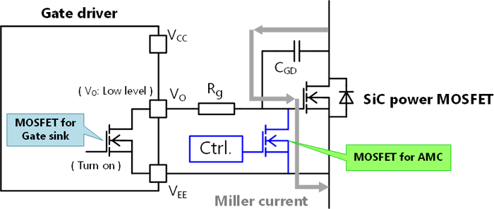
As shown in Figure 1, the Active Miller Clamp is a function to short between the gate-source or gate-emitter during the gate-off period by adding an n-channel MOSFET between the gate-source or gate-emitter of power devices such as SiC power MOSFETs and IGBTs. The added n-channel MOSFET prevents the current passing through the Miller capacitance from flowing through the gate resistance (Rg) of the power device to suppress the rise in the gate voltage. This prevents self-turn-on.

Toshiba provides Smart Gate Driver Coupler TLP5222, TLP5212, TLP5214A with both built-in Active Miller Clamp and built-in short-circuit protection function, as well as TLP5814H with built-in Active Miller Clamp for single gate driver coupler.
This section describes the Active Miller Clamp built in TLP5814H.
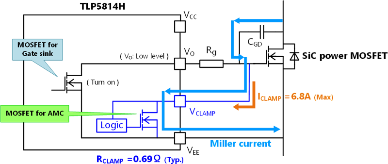
Figure 2 shows the internal circuit of TLP5814H.

The Active Miller Clamp built into TLP5814H operates when the following two conditions are satisfied and short the gate-source or gate-emitter of the power device.
(1) Its gate output voltage (VO terminal voltage) is low.
(2) The gate voltage of the power device (VCLAMP) falls below 2.5V.
The lower the on-resistance of built-in MOSFET for AMC shown in Figure 2, the more effective the Active Miller Clamp is. For TLP5814H, an n-channel MOSFET equivalent to the n-channel MOSFET with the peak-current of 6.8A for gate sink is used for AMC, and the on-resistance is 0.69 Ω (Typ.) at VCLAMP =2.5V.
TLP5814H is suitable for gate driving of SiC power MOSFETs that are sensitive to changes in gate voltage. It is also easy to handle because of the industry-standard 8-pin package, SO8L. It is particularly effective for multi-level inverters where the gate-isolated power supply that doubles the number of uses with power devices and negative bias isolated power supplies cannot be prepared.
For details on the gate positive bias isolated power supplies for the multi-level inverters, refer to the reference design "3-Phase Multi-Level Inverter using MOSFET".
Related Links
The following documents also contain related information.

